

Exit

Author Archives: Kathy Stillman

  1. How Proton Exchange Membranes Benefit from PCM Capabilities

    Comments Off on How Proton Exchange Membranes Benefit from PCM Capabilities

    PCM and PEM Make Electricity

    For engineers and designers developing proton exchange membrane (PEM) fuel cell components, design freedom is tightly linked to performance. Flow-field geometry, current distribution, mass transport, thermal management, corrosion resistance, and cost all compete for priority within extremely tight tolerances. Photo Chemical Machining (PCM) offers a level of design and performance flexibility that is difficult—or impossible—to achieve with conventional fabrication methods such as stamping, laser cutting, or mechanical machining.

    Below are the key ways PCM enables greater flexibility and better-performing PEM components.


    1. True Design Freedom for Complex Flow Fields

    PEM components such as bipolar plates, flow field plates, current collectors, and diffusion layers depend heavily on precise and often intricate geometries. Channel width, depth, pattern complexity, and edge definition directly influence reactant distribution, pressure drop, and water management.

    PCM allows engineers to:

    • Create highly complex, non-linear channel geometries

    • Vary channel widths, land widths, and feature density within a single part

    • Integrate manifolds, micro-features, and transitional geometries without added cost

    Because PCM uses a photolithographic process rather than mechanical force, complexity is essentially “free.” A serpentine, interdigitated, or bio-inspired flow field costs no more to produce than a simple pattern, enabling rapid iteration and performance-driven design optimization.


    2. Burr-Free, Stress-Free Metal Components

    Mechanical cutting and stamping introduce burrs, residual stress, and deformation, all of which can compromise sealing, coating adhesion, and long-term durability in PEM stacks.

    PCM is a non-contact, stress-free process, meaning:

    • No burrs that could damage membranes or seals

    • No work hardening that affects corrosion resistance

    • Flat, distortion-free parts ideal for stacking and gasketing

    This is especially valuable for thin metallic PEM components where even minor distortion can lead to leakage, uneven compression, or reduced efficiency.


    3. Material Flexibility for Corrosion and Performance Needs

    PEM fuel cell environments are chemically aggressive, requiring materials with excellent corrosion resistance and electrical conductivity. PCM supports a wide range of metals commonly used in PEM systems, including:

    • Stainless steels (300 and 400 series)

    • Nickel alloys

    • Other Specialty Metals

    Because PCM does not rely on mechanical tool wear or heat input, material selection is driven by performance—not manufacturability constraints. Engineers can select thinner gauges or more exotic alloys without sacrificing feature resolution or cost efficiency.


    4. Precision at Thin Gauges and Micro-Scale Features

    PEM components often demand thin metal sections with fine features to reduce weight, minimize ohmic losses, and improve thermal response. PCM excels at producing:

    • Ultra-thin metal parts (down to tens of microns)

    • Fine features and tight spacing

    • High feature-to-thickness ratios that are difficult for laser or stamping processes

    This capability enables lightweight stack designs, improved power density, and enhanced thermal and fluid control—key performance drivers in both stationary and mobile fuel cell applications.


    5. Rapid Iteration from R&D to Production

    PEM technology continues to evolve rapidly, and design iteration is critical. PCM uses digital phototools rather than hard tooling, allowing engineers to:

    • Modify designs quickly without expensive die changes

    • Prototype and validate multiple design variants in parallel

    • Transition seamlessly from prototype to low- or mid-volume production

    This agility shortens development cycles, reduces technical risk, and supports continuous performance optimization—particularly important in emerging hydrogen and fuel cell markets.


    6. Functional Integration and Part Consolidation

    PCM enables multiple functions to be integrated into a single metal component. Features such as flow channels, alignment holes, tabs, slots, and electrical contact regions can be etched simultaneously, reducing:

    • Part count

    • Assembly complexity

    • Stack variability and failure points

    For PEM designers, this translates directly into improved reliability, lower system cost, and better overall performance.


    Conclusion

    For engineers and designers of proton exchange membrane components, Photo Chemical Machining offers a rare combination of design freedom, material flexibility, and performance-driven precision. By removing many of the geometric, material, and tooling constraints imposed by conventional fabrication methods, PCM empowers teams to focus on what matters most: optimizing electrochemical performance, durability, and system efficiency.

    In a technology where small design changes can yield significant performance gains, PCM is not just a manufacturing process—it is a strategic enabler of innovation in PEM fuel components.

    For More Information

    Contact

    "*" indicates required fields
    This field is for validation purposes and should be left unchanged.
    Name*
    Please let us know what's on your mind. Have a question for us? Ask away.

  2. PCM and Function-First Design Meet Low Earth Orbit

    Comments Off on PCM and Function-First Design Meet Low Earth Orbit

    PCM Meets Low Earth Orbit

    Designing precision metal components for telecommunication satellites demands a relentless focus on function, reliability, and mass efficiency. Every gram matters, every micron counts, and every material choice must survive extreme thermal cycling, vibration, and radiation exposure. In this environment, photo chemical machining (PCM) offers engineers and designers a powerful advantage: true function-first design freedom. By removing many of the constraints imposed by conventional fabrication methods, PCM enables satellite hardware to be designed around performance requirements rather than manufacturing compromises.

    Designing for Function, Not Tooling

    Traditional metal fabrication processes—such as stamping, punching, or laser cutting—often force designers to adapt their designs to tooling limitations. Minimum feature sizes, tool access, corner radii, burr control, and heat-affected zones all influence how a part must be designed. In contrast, PCM is a tool-less, chemical process that uses photo imaging to define features. This allows engineers to design intricate geometries, tight feature spacing, and complex internal patterns without worrying about tool wear, punch access, or cutting direction.

    For telecommunication satellites, this freedom is especially valuable in components such as RF shields, waveguide elements, antenna structures, grounding fingers, and precision apertures. Engineers can prioritize electromagnetic performance, signal isolation, and frequency control without sacrificing manufacturability.

    Enabling Lightweight, High-Performance Structures

    Weight reduction is a constant objective in satellite design. PCM enables aggressive mass optimization by allowing designers to selectively remove material while maintaining structural integrity. Complex lattice patterns, perforated geometries, and variable feature densities can be etched directly into thin metal sheets with high repeatability.

    This capability supports function-first design by letting engineers tailor stiffness, thermal behavior, and electromagnetic properties within a single component. For example, RF shielding panels can incorporate precise vent patterns that balance EMI suppression with thermal dissipation and outgassing requirements—something difficult or costly to achieve with mechanical machining.

    Preserving Material Properties for Mission Reliability

    Telecommunication satellites rely on materials such as stainless steel, copper alloys, nickel alloys, and specialty metals selected for conductivity, corrosion resistance, and dimensional stability. PCM introduces no mechanical force or thermal energy into the part, eliminating heat-affected zones and residual stresses that can compromise performance.

    This is particularly important for thin-gauge components used in RF paths and electronic assemblies, where flatness, conductivity, and dimensional stability directly affect signal performance. By preserving the base material’s properties, PCM allows engineers to design components purely around electrical and mechanical function rather than compensating for process-induced distortion.

    Supporting Ultra-Fine Features and Tight Tolerances

    As satellite communication systems continue to evolve toward higher frequencies and more compact architectures, feature resolution becomes increasingly critical. PCM excels at producing fine lines, small openings, and precise edge definition across large areas. This makes it ideal for components such as frequency-selective surfaces, encoder disks, shielding grids, and micro-scale alignment features.

    Because PCM etches all features simultaneously, positional accuracy is maintained across the entire part. Engineers can integrate multiple functional elements—mounting features, shielding patterns, and flow paths—into a single component, reducing part count and assembly complexity.

    Accelerating Design Iteration and Innovation

    Satellite programs often involve extensive modeling, testing, and iteration before final designs are locked in. PCM supports rapid design changes by allowing photo tools to be updated quickly and inexpensively compared to hard tooling. Engineers can test multiple design variants—adjusting feature size, spacing, or geometry—without incurring long lead times or high retooling costs.

    This agility encourages innovation and experimentation, enabling teams to optimize performance earlier in the development cycle. For function-first design, this means fewer compromises and greater confidence that the final component truly meets mission requirements.

    From Prototype to Production with Consistency

    Once a design is validated, PCM scales efficiently from prototype quantities to full production. Multiple identical components can be produced in a single etch cycle, ensuring consistency across batches—an essential requirement for satellite constellations and multi-unit deployments.

    Conclusion

    For engineers and designers of precision metal components in telecommunication satellites, photo chemical machining unlocks a level of design freedom that aligns perfectly with function-first engineering. By eliminating many traditional manufacturing constraints, preserving material properties, and enabling rapid iteration, PCM empowers teams to design components that maximize performance, reliability, and efficiency—exactly what space-based communication systems demand.

    For More Information

    Complete Guide to Photo Chemical Machining

    "*" indicates required fields

    This field is for validation purposes and should be left unchanged.

  3. 2025’s Top Ten FAQs about Photo Chemical Machining Applications

    Comments Off on 2025’s Top Ten FAQs about Photo Chemical Machining Applications

    Questions They Want to Know About

    Photo chemical machining (PCM), also known as chemical etching, continues to gain traction across many industries as engineers look for better ways to produce complex, high-precision metal components. In 2025, interest in PCM is being driven by miniaturization, faster product development cycles, and the need for stress-free fabrication. Below are the top ten frequently asked questions about applications for photo chemical machining—and why they matter.


    1. What types of applications are best suited for photo chemical machining?

    PCM is best suited for flat, thin-gauge metal components that require fine detail, tight feature spacing, or complex geometries. Typical applications include electronic shields, precision springs, filters, apertures, encoder disks, lead frames, medical device components, and aerospace shims. Parts that would distort or burr under mechanical cutting are ideal candidates.

    2. Is PCM only used for very small or micro-scale parts?

    No. While PCM excels at producing micro-features, it is equally valuable for larger components that require intricate patterns or tight positional accuracy. Applications range from tiny EMI/RFI shields to large-area metal filtration panels and flow control plates used in energy and industrial systems.

    3. How is PCM used in electronics and electrical applications?

    In electronics, PCM is commonly used to manufacture lead frames, connectors, contact springs, grounding fingers, heat spreaders, and EMI shielding components. Because PCM introduces no heat or mechanical stress, it preserves conductivity and flatness—critical requirements for reliable electronic performance.

    4. Why is PCM popular in aerospace and defense applications?

    Aerospace and defense applications often require thin, lightweight metal parts with exacting tolerances and flawless edges. PCM is used for shims, brackets, thermal management components, screens, and RF components. Its ability to process high-performance alloys without altering material properties makes it especially valuable in these sectors.

    5. Can PCM be used for medical and life science components?

    Yes. PCM is widely used in medical devices and life science equipment for components such as surgical blades, implantable device parts, diagnostic filters, and microfluidic elements. The burr-free edges and high repeatability of PCM help meet strict regulatory and performance requirements.

    6. Is photo chemical machining suitable for metal filtration and flow control?

    Absolutely. PCM is a preferred method for producing precision metal filters, sieves, and flow control plates. Applications include fuel cells, hydraulic systems, medical devices, and industrial filtration. PCM enables consistent hole size, shape, and distribution—key factors in predictable flow performance.

    7. How does PCM support rapid prototyping and product development?

    One of the most common 2025 FAQs is about speed. PCM allows engineers to move from CAD to finished parts in days, not weeks. Design changes are implemented by modifying the photo tool, not expensive hard tooling, making PCM ideal for iterative development and early-stage applications.

    8. What role does PCM play in energy and power applications?

    PCM is increasingly used in power generation, energy storage, and hydrogen technologies. Applications include battery current collectors, fuel cell plates, gas diffusion layers, and sensor components. PCM supports high precision and repeatability while handling corrosion-resistant and exotic alloys common in energy systems.

    9. Can PCM replace stamping, laser cutting, or EDM in certain applications?

    Yes, particularly when applications demand fine features, tight spacing, or distortion-free parts. PCM often outperforms stamping for low-to-medium volumes and complex designs, and it avoids the heat-affected zones associated with laser and EDM processes—making it a better fit for sensitive applications.

    10. How scalable are PCM applications from prototype to production?

    PCM scales efficiently from single prototypes to high-volume production. Multiple identical parts are etched simultaneously from large metal sheets, maintaining consistency across batches. This scalability makes PCM suitable for applications that start in R&D and grow into full production without changing fabrication methods.


    Conclusion

    In 2025, photo chemical machining applications span electronics, aerospace, medical devices, energy systems, and industrial manufacturing. Engineers and designers continue to ask about PCM because it solves many modern fabrication challenges—complex geometry, rapid iteration, material integrity, and scalability. Understanding where PCM excels helps teams apply it strategically, accelerating innovation while maintaining precision and performance.

    For More Information

    Request for Quote

    "*" indicates required fields

    This field is for validation purposes and should be left unchanged.
    Name*
    PCM is best for parts between .001" to .080"
    Drop files here or
    Max. file size: 128 MB.

    • PCM Accelerates Design to Production for Precision Metal Parts

      Comments Off on PCM Accelerates Design to Production for Precision Metal Parts

      Engineers and designers of precision metal components face constant pressure to reduce development cycles, control cost, and deliver increasingly complex geometries without compromising performance. As products become thinner, lighter, and more functionally integrated, conventional metal fabrication methods such as stamping, laser cutting, wire EDM, and fine blanking often impose constraints that slow innovation or inflate cost. Photo chemical machining (PCM), also known as chemical etching, offers a distinct set of capabilities that can be strategically leveraged to enhance both new product development and scaled production.

      Accelerating Early-Stage Product Development

      One of PCM’s greatest strengths is its ability to dramatically shorten the design-to-prototype cycle. Because PCM uses digital phototools rather than hard tooling, engineers can move from CAD data to physical parts in days rather than weeks or months. Design iterations are accomplished by modifying artwork files instead of reworking dies or fixtures, enabling rapid experimentation with geometry, hole patterns, feature density, and material thickness.

      This speed is especially valuable during concept validation and early engineering builds, where designs are still evolving. Engineers can test multiple design variants in parallel—something rarely economical with stamping or fine blanking. The result is faster learning, earlier identification of design risks, and more confident design freeze decisions.

      PCM also allows prototypes to be produced in production-intent materials, including stainless steels, nickel alloys, copper alloys, and specialty metals. This enables more accurate functional testing of electrical, thermal, fluidic, or mechanical performance compared to prototypes made using substitute materials or additive methods.

      Enabling Complex, High-Density Geometries

      As component functionality increases, designers often require intricate features such as fine slots, micro-holes, variable wall thicknesses, and complex internal cutouts. PCM excels at producing these features without introducing mechanical stress, burrs, or heat-affected zones.

      Unlike punching or stamping, PCM does not rely on force, eliminating deformation and residual stress that can distort thin or delicate parts. Unlike laser or EDM processes, it does not generate recast layers or thermal damage that can degrade fatigue life or electrical conductivity. This makes PCM particularly well suited for thin metal components—often from 0.0005″ to 0.060″ thick—where dimensional stability and flatness are critical.

      High-density feature patterns, such as those used in filters, screens, EMI/RFI shielding, fuel cell components, and sensor elements, can be produced with exceptional uniformity across large sheets. Designers can incorporate patterns that would be impractical or cost-prohibitive with mechanical tooling, enabling performance gains without adding assembly steps.

      Supporting Design for Manufacturability (DFM)

      PCM encourages a different approach to design for manufacturability. Because features are created chemically rather than mechanically, designers are freed from many traditional constraints such as minimum punch spacing, tool clearance, or tool wear. This opens opportunities to consolidate parts, eliminate secondary operations, and reduce overall system complexity.

      Engineers who understand PCM design rules—such as etch factor, undercut behavior, and material-thickness relationships—can intentionally design features that take advantage of the process. For example, half-etched features can be used to create bend lines, fluid channels, identification marks, or thickness transitions without secondary machining.

      These capabilities enable more elegant designs that integrate multiple functions into a single component. Fewer parts mean fewer tolerances to stack, fewer failure modes, and lower assembly cost—outcomes that directly support reliability and manufacturability goals.

      De-Risking the Transition to Production

      A common challenge in precision manufacturing is the gap between prototype success and production reality. PCM helps bridge this gap by using the same fundamental process for both prototyping and production. Engineers can validate designs under realistic manufacturing conditions early in the development cycle, reducing the likelihood of late-stage surprises.

      For low-to-medium volume production, PCM can often be the final manufacturing solution, eliminating the need for expensive progressive tooling altogether. Even for higher-volume programs that eventually transition to stamping or fine blanking, PCM is frequently used as a bridge process. It allows products to enter the market sooner while production volumes ramp up and tooling investments are justified.

      Because PCM tooling costs are relatively low, engineers and product managers can make data-driven decisions about when—or whether—to transition to other processes based on real demand rather than forecasts.

      Enhancing Precision Without Over-Specifying Tolerances

      While PCM is not a statistical process control-driven process in the same way as precision machining, it offers consistent, repeatable feature geometry when properly applied. For many functional features—such as flow area, open-area percentage, electrical pathways, or optical patterns—the performance-critical parameter is geometry rather than tight linear tolerances.

      Engineers who focus on functional requirements instead of defaulting to overly tight tolerances often find that PCM delivers exactly what is needed, without paying for unnecessary precision. This mindset shift can reduce cost, improve yield, and align manufacturing capability with actual product performance needs.

      Material Efficiency and Sustainability Benefits

      PCM removes material only where needed, with minimal scrap compared to subtractive machining. The etching chemistry is typically regenerated and recycled within closed-loop systems, and unused sheet material can often be reclaimed. For high-value alloys, this material efficiency can significantly reduce cost.

      Additionally, the absence of mechanical force and heat means less energy consumption per part compared to some alternative processes. As sustainability and lifecycle considerations become more important in product development, PCM can support corporate environmental objectives without sacrificing performance.

      Expanding Design Possibilities Through Collaboration

      To fully leverage PCM, engineers and designers benefit from early collaboration with experienced PCM manufacturers. Process experts can provide guidance on feature sizing, tolerancing strategy, material selection, and panelization approaches that maximize yield and consistency.

      This collaborative approach transforms PCM from a “build-to-print” service into a design-enabling technology. When engineers understand what is possible—and where tradeoffs exist—they can push innovation further while maintaining manufacturability and cost control.

      Conclusion

      Photo chemical machining is far more than a niche fabrication method. When applied strategically, it becomes a powerful tool for accelerating product development, enabling complex designs, reducing manufacturing risk, and supporting efficient production of precision metal components. Engineers and designers who understand and embrace PCM’s unique capabilities can unlock new design freedom, shorten time-to-market, and deliver higher-performing products with fewer compromises.

      In an environment where speed, precision, and adaptability define competitive advantage, PCM offers a proven path to smarter, more agile product development and production.


      For More Information

      Request for Quote

      "*" indicates required fields

      This field is for validation purposes and should be left unchanged.
      Name*
      PCM is best for parts between .001" to .080"
      Drop files here or
      Max. file size: 128 MB.


      • When Precision Demands More: Try Photo Etching

        Comments Off on When Precision Demands More: Try Photo Etching

        When working with precision metal components, many learn that no single fabrication process fits every challenge.

        When tolerances are tight, features are fine, and materials are thin or complex shapes, traditional methods like stamping, punching, or laser and EDM cutting can introduce limitations—mechanical stress, heat distortion, or tooling costs among them. That’s where Photo Chemical Machining (PCM) stands apart.

        Here are six times to consider Photo Etching (PCM by another name):

        1. When the Design Features Are Extremely Fine or Complex

        PCM is a photolithographic process capable of producing intricate profiles, micro features, and complex geometries that would be difficult or impossible to machine or stamp.
        • No mechanical stress: There’s no contact with cutting tools or dies.
        • True-to-design accuracy: Etched features replicate the CAD image exactly, ideal for fine meshes, filters, and precision spring elements.
        • Consistent edge definition: Even on complex or compound shapes.
        Typical features can be as fine as 0.1 mm (0.004 in), with tolerances down to ±0.38 mm depending on thickness.

        2. When Material Integrity Must Be Preserved
        Laser, plasma, and EDM cutting introduce heat-affected zones (HAZ), which can alter metallurgical properties, cause edge hardening, or induce microcracks—issues that are especially critical in aerospace alloys, battery foils, or precision electronic components.
        PCM is a cold process, removing metal chemically rather than thermally. The result:
        • No burrs or recast layers.
        • No stress, deformation, or surface hardening.
        • Uniform material properties across every part.

        3. When Prototyping or Design Iteration Is Frequent
        Because PCM uses photo tooling instead of hard dies, design changes are quick and inexpensive to implement. New patterns can be generated digitally and applied without investing in costly stamping tools or EDM fixturing.
        • Perfect for rapid prototyping or short runs.
        • Seamless transition to full production without retooling delays.
        This flexibility makes PCM especially valuable for R&D programs and for industries under constant innovation pressure—electronics, medical devices, and fuel cell technologies among them.

        4. When Production Volumes Are Moderate to High, but Tooling Budgets Are Tight
        Unlike stamping or punching, PCM requires no expensive, wear-prone dies. Phototools are and inexpensive to reproduce or modify, generally less than $500.
        This not only reduces upfront cost but also eliminates tool wear variables that affect dimensional consistency over long runs.
        5. When Edge Quality and Burr-Free Surfaces Matter

        Mechanical or thermal cutting processes often require secondary finishing to remove burrs, slag, or taper.
        PCM produces parts that are flat, burr-free, and ready for assembly or plating straight from the etching line. This is particularly beneficial in multi-layer laminations, fine filters, and components where post-processing could distort thin materials.

        6. When Working with Thin or Delicate Metals

        Photo chemical machining excels in thin gauge metals (typically 0.001–0.080 inch thick). Stamping or punching thin foils risks distortion or tearing, while lasers can warp small parts through heat input.
        PCM maintains flatness and feature fidelity even in materials like stainless steel, copper, nickel and specialty alloys.

        In Summary
        If your part design demands:
        • Intricate detail
        • No burrs or heat distortion
        • Economical prototyping and fast design iteration
        • Consistent quality across high volumes
        …then Photo Chemical Machining may be the most efficient and precise solution available.
        By integrating PCM early in the design phase, engineers can unlock geometries and tolerances that conventional processes simply can’t match—without sacrificing time, cost, or material performance.

        CONARD’s Free Ebook Design Guide can be Downloaded here:

        Comprehensive Guide to Photochemical Machining

        "*" indicates required fields

        This field is for validation purposes and should be left unchanged.


      • PCM and SPC: Why Never the Twain Shall Meet

        Comments Off on PCM and SPC: Why Never the Twain Shall Meet

        Lies, Da–ed Lies, and Statistics (attributed to Mark Twain)

        In precision manufacturing, process capability indices such as Cpk are widely used to quantify a process’s ability to produce parts within specified tolerance limits. A Cpk of 1.33 or greater is often considered the benchmark for a capable and statistically controlled process. However, photo chemical machining (PCM)—while unmatched for producing intricate, burr-free metal components—does not conform neatly to the same statistical models that define conventional, mechanically driven manufacturing processes. The reason lies in the very nature of PCM as a chemical and photolithographic process, where dimensional outcomes are influenced by multiple variables that cannot be reduced to consistent mechanical relationships.

        The Nature of PCM and Its Process Variables

        Photo chemical machining removes metal by chemical dissolution through patterned photoresist masks. Each step—cleaning, coating, imaging, developing, etching, and stripping—introduces variations that stem from chemical kinetics, fluid dynamics, and photoresist behavior rather than from mechanical repeatability. While these steps are highly controlled, their outputs inherently exhibit non-linear variability.

        Key sources of variation include:

        • Etchant composition and temperature: Small fluctuations in chemical concentration, temperature, and flow rate alter the metal removal rate. Even under careful control, these parameters drift over time due to etchant depletion and reaction byproducts.
        • Photoresist coating thickness and exposure: Variations in resist thickness or UV exposure energy affect pattern fidelity, especially along fine features and sharp corners.
        • Undercut geometry: Because etching attacks both vertically and laterally, the final feature size is affected by etch depth and time in a non-linear way that depends on alloy composition, sheet thickness, and feature density.

        These are systemic chemical variations, not random or assignable mechanical errors. Therefore, the output distribution for etched dimensions is rarely normal (bell-shaped), a fundamental assumption behind statistical process control metrics such as Cpk.

        Cpk Assumes Mechanical Repeatability

        In machining, stamping, or molding, dimensional variation follows predictable physical laws—tool wear, press stroke consistency, thermal expansion, or machine alignment. Once the sources of variation are minimized and stable, the process can be characterized statistically with high confidence.

        A Cpk of 1.33 means that the process variation (6σ spread) comfortably fits within the specification limits with a central mean. In other words, both the distribution and its stability are measurable and repeatable.

        In PCM, however, the distribution of results from etching is not normally distributed and not constant over time. The process behaves more like controlled corrosion than mechanical removal. While etch rate can be closely monitored, small environmental or material variations can shift feature sizes by several microns in unpredictable directions. That makes it impossible to apply the same statistical confidence intervals as one would with cutting tools or stamping dies.

        Dimensional Control Without Cpk

        Despite its inability to demonstrate a Cpk of 1.33, PCM consistently meets demanding dimensional tolerances—often in the range of +/-10% of material thickness or better—by using process modeling, empirical calibration, and in-process measurement. Manufacturers routinely measure test coupons or witness samples on every panel to monitor etch rate and adjust dwell time dynamically.

        Instead of relying on statistical control charts, PCM achieves precision through feedback control and process compensation. For example, artwork dimensions are adjusted (“compensated”) to offset expected undercut or over-etch, ensuring that final part geometries meet design intent even if the chemical variation is not statistically stable.

        This approach is deterministic rather than statistical. The process may not achieve a Cpk of 1.33, but it consistently produces parts within tolerance by design.

        Conclusion

        Photo chemical machining defies the conventional assumptions that make statistical process control meaningful. Its core variables—chemical concentration, temperature, photoresist behavior, and etch kinetics—introduce complex, non-normal variation that cannot be stabilized to the degree required for a Cpk of 1.33.

        However, this does not reflect a lack of precision or quality. Instead, it highlights that PCM is governed by chemical control rather than mechanical predictability. Manufacturers ensure precision through real-time monitoring, empirical correction, and deep process expertise—not through statistical metrics designed for mechanically repeatable systems.

        In short, PCM is a capable process, but not a statistically capable process in the SPC sense. Its precision arises from science and control, not statistics and normality.

        For More Information

      • PCM and DPG– Distributed Power Generation: Made for Each Other

        Comments Off on PCM and DPG– Distributed Power Generation: Made for Each Other

        Distributed power generation (DPG) has become a central pillar of modern energy strategy, driven by the need for efficiency, resiliency, and the integration of low-carbon technologies. Instead of relying solely on large, centralized plants, distributed systems leverage smaller units such as fuel cells, microturbines, solar arrays, wind and advanced nuclear technologies like pressurized water reactors (PWRs) designed for modular or microgrid deployment. Within this evolving landscape, photo chemical machining (PCM) plays an important role by enabling the precise fabrication of critical metal components that directly impact efficiency, safety, and reliability.

        Why PCM Matters in Distributed Power Systems

        DPG technologies demand components that are both highly precise and optimized for thermal and fluid performance. Unlike conventional power plants, distributed units often operate at smaller scales, where every increment of efficiency translates into meaningful gains. At the same time, these technologies must balance compactness with durability under extreme operating conditions, such as high pressure, high temperature, or corrosive environments.

        PCM, sometimes called photo etching or photochemical etching, is uniquely suited to this challenge. It allows engineers to manufacture intricate patterns in thin metal foils and sheets without mechanical stress or heat distortion. Because the process uses a photoresist mask and chemical etchants, it can create highly detailed geometries with tolerances in the range of ±50–100 microns. This precision enables designers to develop complex flow channels, fine filters, and lightweight heat transfer structures that would be difficult or prohibitively expensive to achieve with stamping, laser cutting, or wire EDM.

        Applications in Fuel Cells and Microturbines

        Fuel cells, a cornerstone of distributed energy systems, rely on repeating units of bipolar plates or proton exchange membrane (PEM) elements. PCM enables the manufacture of these plates with intricate micro-channel patterns for optimized gas flow, water management, and thermal regulation. Since the process leaves no burrs or recast layers, the risk of short circuits or localized stress points is eliminated, directly improving stack reliability.

        Microturbines, which generate power from gaseous or liquid fuels, also benefit from PCM in the production of filtration screens, precision orifices, and flow restrictors. These components govern the efficient mixing of air and fuel, protect turbine blades from particulates, and help optimize combustion. PCM’s capability for producing thousands of identical parts at scale further aligns with the economic requirements of distributed power adoption.

        Pressurized Water Reactors in Distributed Power

        Perhaps the most exciting development in distributed power is the emergence of small modular reactors (SMRs), particularly those based on pressurized water reactor technology. Traditional PWRs are the backbone of large-scale nuclear generation, but SMRs adapt this proven design into smaller, factory-fabricated modules suitable for distributed deployment. Here again, PCM plays a critical role.

        In SMRs and advanced PWRs, thermal efficiency depends on highly controlled coolant flow, effective heat transfer surfaces, and robust filtration of particulates or corrosion products. PCM can produce finely tuned flow plates, micro-channel heat exchangers, and support grids for reactor internals that meet the tight tolerances demanded by nuclear applications. Because the process avoids mechanical stress, the integrity of specialty alloys such as Inconel or stainless steels—commonly used in nuclear systems—is preserved. This ensures long-term resistance to radiation, pressure, and chemical attack.

        Moreover, nuclear safety places a premium on component uniformity and reliability. PCM’s repeatability supports the production of critical safety-related parts without variability that could compromise performance. For modular PWRs, where standardization and scalability are essential to economic deployment, PCM provides a manufacturing pathway aligned with industry goals.

        Enabling Innovation and Integration

        Beyond specific technologies, PCM supports innovation across distributed power generation by freeing engineers from many of the geometric limitations imposed by subtractive machining or forming. Designers can iterate more quickly, experiment with new flow-field architectures, or integrate multifunctional features into a single etched plate. This design flexibility accelerates the development of more compact, efficient, and durable distributed power units.

        Conclusion

        Distributed power generation technologies are reshaping how energy is produced and consumed. From fuel cells and microturbines to modular pressurized water reactors, success depends on components that combine precision, durability, and efficiency. Photo chemical machining provides the capability to manufacture such parts at scale while preserving material integrity and enabling innovative designs. Its role is not merely supportive but foundational, helping to ensure that the next generation of distributed energy systems meets the demands of performance, safety, and sustainability.

        For More Information on Photo Chemical Machining

        Contact

        "*" indicates required fields

        This field is for validation purposes and should be left unchanged.
        Name*
        Please let us know what's on your mind. Have a question for us? Ask away.

      • How PCM Helps Designers and Engineers Meet Technology-driven Design Goals

        Comments Off on How PCM Helps Designers and Engineers Meet Technology-driven Design Goals

        Technology driven design

        We talk to dozens of engineers and designers who are looking for new ways to solve their most challenging design efforts. Sometimes, the parts they want to make are too complex for the processes they’re accustomed to using. Other times, they need parts in batch sizes that are impractical for other fabrication methods: perhaps too few for stamping or too many for laser.

        Photo chemical machining has characteristics that make it an effective option for some of these problems. Here are four benefits that engineers and designers should know about:

        “At its hottest point, the etching process reaches temperatures of about 125℉. “

        No stresses or deformations on the finished part

        The cutting- and stamping-based fabrication methods are more well-known, but they have some shortcomings that give designers pause. For example, laser cutting and wire EDM exposes the workpiece to extremely high temperatures, leading to heat affected zones or recast layers that can change the characteristics of the metal alloy.  Stamping and punching can create work hardening that requires remediation through annealing. Stamping and CNC milling can lead to mechanical distortions, burrs and uneven edges.

        Photo etching has none of these problems. At its hottest point, the etching process reaches temperatures of about 125℉. And because the parts are chemically etched out of the sheet metal, there are no cutting or shearing actions that lead to burrs or other deformations.

        Well-suited for complex geometries and features on flat parts

        Today, screens, meshes, sieves and other parts that require many small holes or design features are finding their place in industrial, medical, electronic and scientific applications. For most of the conventional fabrication processes, these parts are either nearly impossible to make, or are completely impractical in terms of tooling, cycle time or costs.

        A phototool is a stencil used to imprint the pattern of the parts on the metal. All of the features, including as many holes as may be needed, are etch all at once at no additional cost. This saves time and ensures the uniformity of each hole on the part. The photo etching process produces consistent, burr-free holes as small as 0.004″ in 0.002″ thick material. As a rule, minimum hole size is 110 percent of the thickness of the material. On 0.010″ thick material, the smallest hole we could make would be 0.011″.

        Designers and engineers today need precise component parts and are looking for new processes that help them solve design problems.

        Tight, consistent tolerances are built in

        The phototool is extremely accurate because light is its only working exposure. Thus, there is there is no “tool wear” that could lead to tolerance variations. Because of this, the locational tolerances for design features generally meet the nominal dimensions of the specification.

        Dimensional tolerances are dictated by the thickness of the metal. We can typically hold these to within +/-15% of the sheet’s thickness.

        Design changes are quick and easy

        Phototools are inexpensive, generally about $400 and can be made in about 2 days. This means that designers can change their designs without incurring substantial costs or delays.

        For detailed information, our newly updated Comprehensive Guide to Photo Chemical Machining offers engineers and designers technical information to assist their projects:


        Check out the “Minutes with Max” video series.  All about etching in bite-size chunks.

        Got a Question?

      • Comparing Metal Fabricating Options

        Comments Off on Comparing Metal Fabricating Options

        Options for Fabricating Precision Metal Components


        Modern solid modeling systems offer very direct paths for outputting data files for laser cutting (and its cousins: water jet and plasma), Wire EDM and even die design for both progressive and single strike die-stamping.  But for sheet metal fabricating’s “best-kept secret,” CAD consideration for photo chemical machining (PCM) is an afterthought.

        PCM, though, offers capabilities and advantages over other processes, if only more engineers and designers knew about them:

        • Processing very thin foils down to .001, even in dead soft aluminum.
        • Metal filtration, grids, screens, apertures (lots of holes), with openings as small as .005”
        • No mechanical or thermal deformations, such as cold working, burrs, heat affected zones or recast layers.

        Here is more information on these fabrication choices:

        1. Stamping

        Overview:

        Stamping is a high-speed process that uses mechanical or hydraulic presses and custom-designed dies to shape or cut sheet metal. It encompasses a variety of techniques including blanking, punching, bending, embossing, and coining.

        Suitable Materials:

        • Steel (carbon, stainless)
        • Aluminum
        • Brass
        • Copper
        • Titanium
        • Specialty alloys

        Process Characteristics:

        • Tooling: Requires hardened steel dies and punches
        • Speed: Very high—ideal for mass production
        • Precision: ±0.01 mm or better with proper tooling
        • Thickness Range: Typically 0.005″ to 0.250″ (0.13 mm to 6.35 mm), depending on material and part size
        • Minimum Feature Size: Limited by die capabilities; sharp internal corners may be difficult
        • Setup Time: High (due to die design and testing)
        • Lead Time: Weeks for tooling; fast production once set up

        Advantages:

        • Exceptional production speed and cost-effectiveness at high volumes
        • Consistent quality and repeatability
        • Capable of complex 3D forms through progressive dies
        • Long tool life with proper maintenance

        Limitations:

        • High initial tooling cost and long lead time
        • Not economical for small batches or prototyping
        • Design changes require costly die modifications
        • Burrs and deformation may occur in thin or soft metals

        Best Applications:

        • Automotive components
        • Connectors and terminals
        • Electronic enclosures
        • Battery contacts
        • High-volume appliance parts
        1. Laser Cutting

        Overview:

        Laser cutting uses a focused laser beam to melt, burn, or vaporize material along a programmed path. CNC systems control the movement of the laser head and material.

        Suitable Materials:

        • Most metals, including steel, aluminum, copper, brass, and titanium
        • Reflective materials require special lasers (e.g., fiber lasers)

        Process Characteristics:

        • Tooling: No physical tooling; requires digital CAD files
        • Speed: Moderate to high (depends on material thickness and complexity)
        • Precision: ±0.025 mm or better
        • Thickness Range: Typically up to 20 mm for steel; thinner foils also supported
        • Minimum Feature Size: ~0.1 mm, depending on laser beam width
        • Setup Time: Very low
        • Lead Time: Short—ideal for prototypes and low to medium volumes

        Advantages:

        • Excellent precision and edge quality
        • High flexibility—easy to modify designs
        • Minimal physical contact reduces distortion
        • No tooling costs—ideal for prototypes or frequent design changes

        Limitations:

        • Heat-affected zones (HAZ) may cause microstructural changes or warping
        • Not ideal for very thick metals or parts requiring tight tolerances over long runs
        • Slower than stamping for large production volumes
        • May leave oxide layers or require post-processing

        Best Applications:

        • Prototypes and short-run components
        • Decorative or complex cutouts
        • Medical device parts
        • Aerospace brackets
        • Custom enclosures
        1. Photo Chemical Machining (PCM)

        Overview:

        Photo chemical machining (also called photo etching or chemical machining) involves coating the metal with a photoresist, exposing it to a patterned UV light source, and etching away exposed areas using acid solutions. This process is especially suited for thin metal parts requiring intricate detail.

        Suitable Materials:

        • Stainless steel
        • Carbon and silicon steels
        • Nickel and many nickel alloys
        • Copper and copper alloys
        • Aluminum
        • Beryllium copper
        • Molybdenum
        • Silver
        • Aluminum and Nickel Braze foils
        • Metal-Clad substrates for flex circuits, resistive heating elements and direct-bond copper

        Check out more options here.

        Process Characteristics:

        • Tooling: Photomasks produced from CAD designs, generally less than $500
        • Speed: Moderate (includes chemical processing time)
        • Precision: ±0.04mm (or better with optimized parameters)
        • Thickness Range: 0.0005″ to 0.060″ (0.013 mm to 1.5 mm)
        • Minimum Feature Size: ~0.06 mm; aspect ratio dependent
        • Setup Time: Moderate (requires photo tooling and chemical baths)
        • Lead Time: ~4 weeks typical

        Advantages:

        • No mechanical or thermal stress on material—ideal for delicate foils
        • Extremely fine detail possible; excellent for micro-scale geometries
        • Burr-free parts with smooth edges
        • Can process multiple parts simultaneously from large sheets

        Limitations:

        • Steel and Nickel alloys up to .040”; copper alloys up to .065” and aluminum up to.080”
        • Titanium and a number of “super alloys” that are very corrosion resistant may require the use of hydrofluoric etching solution.
        • Even with all aqueous chemistries and on-site water treatment, spent solutions and resist are considered hazardous waste and must be handled per regulations.
        • Equipment capacity generally defines maximum sheet sizes, rarely larger than 30” x 60.”

        Best Applications:

        • EMI/RFI shielding
        • Bus bars
        • Lead frames
        • Encoders and precision apertures
        • Fuel cell plates
        • Medical screens and mesh components
        • Battery Components
        • Heat Exchangers
        • Cold Plates
        • Braze Foils
        • Metal Filtration Elements
        • Hermetic lids, flat and stepped
        • Metal shims, gaskets, retainers and seals
        • Flat springs and flexures
        • Scientific and industrial instruments and tools
        1. Wire EDM (Electrical Discharge Machining)

        Overview:

        Wire EDM is a non-contact machining process that uses a continuously fed thin wire and electrical discharges (sparks) to cut conductive metals submerged in dielectric fluid.

        Suitable Materials:

        • Any electrically conductive metal: tool steel, titanium, aluminum, Inconel, tungsten, etc.

        Process Characteristics:

        • Tooling: Requires CAD/CAM programming, but no physical dies
        • Speed: Slow (especially on thick or complex geometries)
        • Precision: Exceptional—±0.002 mm or better
        • Thickness Range: 0.1 mm up to 300 mm+
        • Minimum Feature Size: Wire diameter limited (~0.02–0.3 mm); internal corners have small radii
        • Setup Time: Low to moderate
        • Lead Time: Moderate; often longer than laser/PCM for same part

        Advantages:

        • Capable of extremely tight tolerances and fine finishes
        • Excellent for hard or exotic materials
        • No mechanical force—no warping or distortion
        • Capable of complex internal geometries

        Limitations:

        • Slow cutting speed—not economical for large batches
        • Limited to conductive materials
        • Wire path requires start hole (pre-drilling needed in some cases)
        • High energy consumption per part

        Best Applications:

        • Precision tooling and dies
        • Aerospace and medical implants
        • Microfluidic components
        • Fine gears and intricate mechanical parts
        • Prototyping high-tolerance conductive parts


        Selecting the Right Process

        Choosing the right process depends on several critical factors:

        1. Volume and Cost
        • Stamping is ideal for high-volume production due to its speed and low per-part cost after tooling.
        • Laser cutting and PCM offer more flexibility and lower setup costs, better suited for small to medium batches or frequent design iterations.
        • Wire EDM is best reserved for small-batch, high-precision work due to slower cycle times and higher per-part costs.
        1. Part Complexity and Precision
        • For intricate, burr-free, and stress-free parts from thin foils, PCM excels.
        • When tight tolerances and internal features are critical, wire EDM is unmatched.
        • Laser cutting handles most 2D geometries with good accuracy, while stamping shines in complex 3D forming through progressive dies.
        1. Material Considerations
        • Wire EDM works on any conductive metal, regardless of hardness.
        • Few PCM facilities use HF etching chemistry. Most alloys etch well in Fe3Cl.
        • Laser cutting and stamping accommodate a wide range of alloys.
        1. Time-to-Market and Prototyping
        • Laser cutting and PCM offer the shortest lead times with minimal tooling, making them ideal for prototypes.
        • Stamping is less suitable for early design validation due to tooling investment.
        • Wire EDM, while slower, is useful for prototype-quality parts needing extreme precision.

        Conclusion

        Each of the four fabrication processes—stamping, laser cutting, photo chemical machining, and wire EDM—has its strengths and ideal applications. The choice between them should be guided by a careful balance of design complexity, tolerance requirements, material selection, volume needs, and budget.

        • Use stamping for high-speed, high-volume production where initial tooling investment can be amortized.
        • Choose laser cutting for flexible, quick-turn manufacturing with moderate tolerances.
        • Opt for PCM when producing thin, intricate, burr-free components with tight tolerances.
        • Rely on wire EDM for low-volume, highly complex parts that require exceptional precision and finish.

        Selecting the right process can dramatically affect the efficiency, cost, and quality of your final product—making this decision a cornerstone of successful component manufacturing.

        For more Information:


      • 6 Advantages of Photo Chemical Machining for Metal Filtration Devices

        Comments Off on 6 Advantages of Photo Chemical Machining for Metal Filtration Devices

        The Benefits of Photo Chemical Machining for Metal Filtration Devices

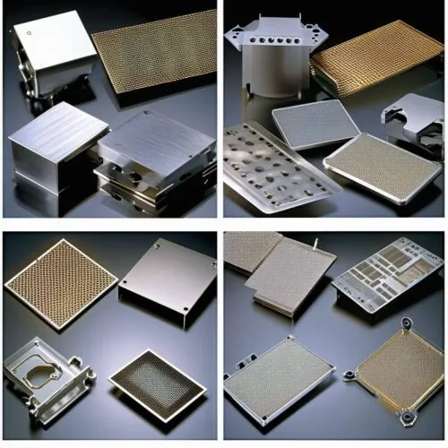
        a variety of photo etched metal parts
        Metal filtration devices play a crucial role in industries ranging from aerospace and automotive to medical, chemical processing, and energy production. These components often require intricate, high-precision perforations and complex geometries to meet functional and performance demands. For manufacturers and design engineers seeking both precision and production efficiency, photo chemical machining (PCM) presents a compelling fabrication method. PCM offers a range of benefits that make it especially well-suited to producing metal filtration devices, including design flexibility, tight tolerances, cost-effectiveness, and superior edge quality.


        1. Unmatched Design Flexibility

        One of the primary advantages of photo chemical machining for filtration components is its ability to create highly intricate and complex patterns in thin metal sheets without the constraints imposed by mechanical tooling. Filters often require thousands—or even millions—of uniform openings, some in custom or non-standard shapes, aligned precisely for fluid or gas flow control.

        PCM uses a photomask and chemical etchants to dissolve unwanted metal areas, allowing for:

        • Free-form geometries (slots, grids, hexagonal, elliptical, or irregular apertures)

        • Complex aperture patterns that would be difficult or impossible with stamping or drilling

        • Micro-scale features with consistent repeatability

        Because PCM is a mask-based process, design changes can be implemented quickly and inexpensively by simply modifying the phototool—without the need for costly retooling or mechanical adjustments. This is particularly beneficial during prototyping or low-to-medium volume production runs, where agility and customization are key.


        2. Tight Tolerances and Dimensional Accuracy

        High-performance filtration systems depend on predictable and uniform aperture sizes to ensure consistent flow rates, pressure drops, and separation performance. PCM is capable of achieving fine feature resolution—often in the range of ±0.025 mm (±0.001 inch) or better—while maintaining flatness and structural integrity of the metal.

        Unlike traditional punching or laser processes, PCM does not introduce mechanical or thermal stress to the material. There is no tool pressure, heat-affected zone, or deformation around the cut areas, which means:

        • Apertures maintain their shape and spacing precisely

        • Parts remain flat and free from burrs or warping

        • Thin metals as light as 0.0005 inches can be accurately machined

        Such precision is critical in medical, fuel cell, or aerospace applications where even slight deviations in pore size can affect system performance or safety.


        3. Burr-Free Edges and Superior Surface Quality

        Filtration components, especially those used in sensitive applications like fluid or gas purification, demand clean and smooth aperture edges to prevent particle retention, bacterial buildup, or flow disruption. Mechanical punching or laser cutting can leave burrs, sharp edges, or recast layers that compromise performance and require secondary finishing.

        In contrast, photo chemical machining is a non-contact, non-thermal process:

        • No mechanical burrs are formed

        • No edge deformation or micro-cracks

        • No heat-affected zone or metallurgical changes

        This results in high-quality surface finishes that meet or exceed industry standards without the need for secondary deburring or polishing operations, reducing overall processing time and cost.


        4. Material Versatility

        Photo chemical machining supports a wide range of metals used in filter applications, including stainless steel, nickel alloys, copper, brass, aluminum, and titanium. The process is especially well-suited to thin metals (typically from 0.0005 to 0.060 inches), and its chemical nature means that hard or exotic materials are no more difficult to machine than softer ones.

        This versatility enables PCM to support a diverse set of filtration solutions, including:

        • EMI/RFI shielding screens

        • Mesh or grid-type fuel injector filters

        • Blood filtration membranes

        • Chemical processing sieves and diffusers

        Additionally, multiple metals can be processed in parallel using similar tooling, which is useful for multi-material filter assemblies or hybrid system designs.


        5. Cost-Effectiveness for Prototyping and Production

        Unlike stamping or EDM, PCM does not require expensive hard tooling. The phototool—a film used to expose the metal—is inexpensive and fast to produce, often in a matter of hours. This makes photo chemical machining ideal for:

        • Rapid prototyping with production-quality results

        • Small-to-medium production runs

        • Low product development cost and faster iteration cycles

        Even in high-volume applications, PCM remains cost-competitive due to its ability to etch multiple parts per sheet simultaneously (nesting), and its reduced need for post-processing.


        6. Scalability and Repeatability

        Once a design is finalized, PCM offers excellent repeatability and scalability. Parts are consistently replicated with high precision and virtually no variation across large production batches. Process control, automation, and mask-based exposure ensure that each part conforms to exacting specifications, reducing waste and increasing yield.


        Conclusion

        For engineers and designers of metal filtration devices, photo chemical machining offers a compelling combination of precision, design freedom, material compatibility, and cost control. Whether you’re developing micro-perforated fuel filters, surgical screens, or high-flow industrial sieves, PCM provides the capability to fabricate complex features reliably, burr-free, and to exact specifications—all while maintaining the flexibility to adapt to evolving designs or production demands.

        In a world increasingly dependent on clean, efficient, and precise filtration systems, photo chemical machining stands out as an advanced manufacturing solution that enables innovation without compromising quality.

        For More Information: