Photo Chemical Machining for Thermal Management Devices
As power densities increase across electronics, energy systems, aerospace platforms, and industrial equipment, thermal management has become a primary design constraint. Engineers are challenged to move heat faster, more efficiently, and within ever-shrinking envelopes—often while meeting aggressive weight, reliability, and materials requirements.
Photo chemical machining (PCM)—also known as photo chemical etching or chemical milling—enables the production of high-precision metal components for thermal management devices that outperform parts made by conventional fabrication methods.
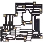
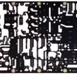
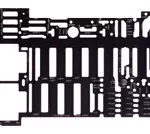
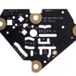
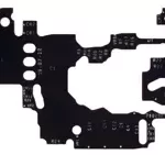
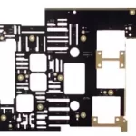
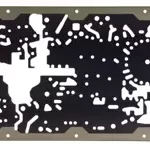
In the example pictured below, about 2,000 etched pin fins increase the effective surface area by nearly 25%. This particular plate, photo-etched in aluminum and used on the space shuttles, has radiating surfaces on both sides.
THERMAL CONDUCTIVITY OF MATERIALS
- Thermal conductivity is expressed in watts/meter*Kelvin (W/m*K).
- Pure aluminum (1100 series) is 247
- Copper is 398,
- Silver is 428
- Diamond is an astounding 2500 watts
Alloying and temper will affect thermal conductivity.
All other things being equal, a copper device will be three times heavier than an aluminum one.
CONARD’S ETCHING RANGE
- Aluminum up to .080” thick
- Copper up to .063” thick.
Locational tolerances, regardless of material thickness will be +/-.001” to drawing nominal. Dimensional tolerances at .063” will run +/-.012” and up to +/-.016″ at .080″.
APPLICATIONS FOR ETCHED THERMAL DEVICES
Precision Heat Exchangers
Modern heat exchangers demand fine, repeatable flow paths to maximize surface area while minimizing pressure drop. PCM enables the fabrication of:
- Micro-channel and multi-channel plates
- Thin-wall fins and louvers
- Stacked etched plates for diffusion bonding or brazing
- Turbulence-enhancing features for improved heat transfer
Cold Plates for Electronics and Power Systems
Cold plates are essential for managing heat in high-power electronics, EV power modules, data centers, and defense systems. Photo chemical machining supports cold plate designs that require:
- Complex internal flow paths
- Ultra-thin walls for efficient heat extraction
- Tight flatness tolerances for thermal interface contact
- Multi-material assemblies
High-Efficiency Heat Sinks
Heat sinks are evolving beyond simple extrusions. PCM enables next-generation heat sink designs with:
- Ultra-thin, high-density fins
- Variable fin spacing for airflow optimization
- Integrated mounting features
- Lightweight metal geometries
Materials Optimized for Thermal Performance
Conard photo chemically machines a wide range of metals commonly used in thermal management, including:
- Copper and copper alloys
- Aluminum and aluminum alloys
- Stainless steels
- Nickel alloys
- Specialty metals for extreme environments
Why Engineers Choose Conard for PCM Thermal Solutions
At Conard, photo chemical machining is more than a process—it’s a design-enabling capability. Our engineers collaborate closely with customers to optimize part geometry, material selection, and downstream joining methods.
What sets Conard apart:
- Decades of PCM expertise
- Application-driven engineering support
- Tight process control for thermal-critical components
- Seamless integration with brazing, bonding, and forming
We don’t just make parts—we help solve thermal problems. Contact us today to learn more.
