Options for Fabricating Precision Metal Components
Modern solid modeling systems offer very direct paths for outputting data files for laser cutting (and its cousins: water jet and plasma), Wire EDM and even die design for both progressive and single strike die-stamping. But for sheet metal fabricating’s “best-kept secret,” CAD consideration for photo chemical machining (PCM) is an afterthought.
PCM, though, offers capabilities and advantages over other processes, if only more engineers and designers knew about them:
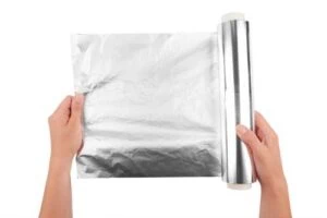
- Processing very thin foils down to .001, even in dead soft aluminum.
- Metal filtration, grids, screens, apertures (lots of holes), with openings as small as .005”
- No mechanical or thermal deformations, such as cold working, burrs, heat affected zones or recast layers.
Here is more information on these fabrication choices:
- Stamping
Overview:
Stamping is a high-speed process that uses mechanical or hydraulic presses and custom-designed dies to shape or cut sheet metal. It encompasses a variety of techniques including blanking, punching, bending, embossing, and coining.
Suitable Materials:
- Steel (carbon, stainless)
- Aluminum
- Brass
- Copper
- Titanium
- Specialty alloys
Process Characteristics:
- Tooling: Requires hardened steel dies and punches
- Speed: Very high—ideal for mass production
- Precision: ±0.01 mm or better with proper tooling
- Thickness Range: Typically 0.005″ to 0.250″ (0.13 mm to 6.35 mm), depending on material and part size
- Minimum Feature Size: Limited by die capabilities; sharp internal corners may be difficult
- Setup Time: High (due to die design and testing)
- Lead Time: Weeks for tooling; fast production once set up
Advantages:
- Exceptional production speed and cost-effectiveness at high volumes
- Consistent quality and repeatability
- Capable of complex 3D forms through progressive dies
- Long tool life with proper maintenance
Limitations:
- High initial tooling cost and long lead time
- Not economical for small batches or prototyping
- Design changes require costly die modifications
- Burrs and deformation may occur in thin or soft metals
Best Applications:
- Automotive components
- Connectors and terminals
- Electronic enclosures
- Battery contacts
- High-volume appliance parts
- Laser Cutting
Overview:
Laser cutting uses a focused laser beam to melt, burn, or vaporize material along a programmed path. CNC systems control the movement of the laser head and material.
Suitable Materials:
- Most metals, including steel, aluminum, copper, brass, and titanium
- Reflective materials require special lasers (e.g., fiber lasers)
Process Characteristics:
- Tooling: No physical tooling; requires digital CAD files
- Speed: Moderate to high (depends on material thickness and complexity)
- Precision: ±0.025 mm or better
- Thickness Range: Typically up to 20 mm for steel; thinner foils also supported
- Minimum Feature Size: ~0.1 mm, depending on laser beam width
- Setup Time: Very low
- Lead Time: Short—ideal for prototypes and low to medium volumes
Advantages:
- Excellent precision and edge quality
- High flexibility—easy to modify designs
- Minimal physical contact reduces distortion
- No tooling costs—ideal for prototypes or frequent design changes
Limitations:
- Heat-affected zones (HAZ) may cause microstructural changes or warping
- Not ideal for very thick metals or parts requiring tight tolerances over long runs
- Slower than stamping for large production volumes
- May leave oxide layers or require post-processing
Best Applications:
- Prototypes and short-run components
- Decorative or complex cutouts
- Medical device parts
- Aerospace brackets
- Custom enclosures
- Photo Chemical Machining (PCM)
Overview:
Photo chemical machining (also called photo etching or chemical machining) involves coating the metal with a photoresist, exposing it to a patterned UV light source, and etching away exposed areas using acid solutions. This process is especially suited for thin metal parts requiring intricate detail.
Suitable Materials:
- Stainless steel
- Carbon and silicon steels
- Nickel and many nickel alloys
- Copper and copper alloys
- Aluminum
- Beryllium copper
- Molybdenum
- Silver
- Aluminum and Nickel Braze foils
- Metal-Clad substrates for flex circuits, resistive heating elements and direct-bond copper
Process Characteristics:
- Tooling: Photomasks produced from CAD designs, generally less than $500
- Speed: Moderate (includes chemical processing time)
- Precision: ±0.04mm (or better with optimized parameters)
- Thickness Range: 0.0005″ to 0.060″ (0.013 mm to 1.5 mm)
- Minimum Feature Size: ~0.06 mm; aspect ratio dependent
- Setup Time: Moderate (requires photo tooling and chemical baths)
- Lead Time: ~4 weeks typical
Advantages:
- No mechanical or thermal stress on material—ideal for delicate foils
- Extremely fine detail possible; excellent for micro-scale geometries
- Burr-free parts with smooth edges
- Can process multiple parts simultaneously from large sheets
Limitations:
- Steel and Nickel alloys up to .040”; copper alloys up to .065” and aluminum up to.080”
- Titanium and a number of “super alloys” that are very corrosion resistant may require the use of hydrofluoric etching solution.
- Even with all aqueous chemistries and on-site water treatment, spent solutions and resist are considered hazardous waste and must be handled per regulations.
- Equipment capacity generally defines maximum sheet sizes, rarely larger than 30” x 60.”
Best Applications:
- EMI/RFI shielding
- Bus bars
- Lead frames
- Encoders and precision apertures
- Fuel cell plates
- Medical screens and mesh components
- Battery Components
- Heat Exchangers
- Cold Plates
- Braze Foils
- Metal Filtration Elements
- Hermetic lids, flat and stepped
- Metal shims, gaskets, retainers and seals
- Flat springs and flexures
- Scientific and industrial instruments and tools
- Wire EDM (Electrical Discharge Machining)
Overview:
Wire EDM is a non-contact machining process that uses a continuously fed thin wire and electrical discharges (sparks) to cut conductive metals submerged in dielectric fluid.
Suitable Materials:
- Any electrically conductive metal: tool steel, titanium, aluminum, Inconel, tungsten, etc.
Process Characteristics:
- Tooling: Requires CAD/CAM programming, but no physical dies
- Speed: Slow (especially on thick or complex geometries)
- Precision: Exceptional—±0.002 mm or better
- Thickness Range: 0.1 mm up to 300 mm+
- Minimum Feature Size: Wire diameter limited (~0.02–0.3 mm); internal corners have small radii
- Setup Time: Low to moderate
- Lead Time: Moderate; often longer than laser/PCM for same part
Advantages:
- Capable of extremely tight tolerances and fine finishes
- Excellent for hard or exotic materials
- No mechanical force—no warping or distortion
- Capable of complex internal geometries
Limitations:
- Slow cutting speed—not economical for large batches
- Limited to conductive materials
- Wire path requires start hole (pre-drilling needed in some cases)
- High energy consumption per part
Best Applications:
- Precision tooling and dies
- Aerospace and medical implants
- Microfluidic components
- Fine gears and intricate mechanical parts
- Prototyping high-tolerance conductive parts
Selecting the Right Process
Choosing the right process depends on several critical factors:
- Volume and Cost
- Stamping is ideal for high-volume production due to its speed and low per-part cost after tooling.
- Laser cutting and PCM offer more flexibility and lower setup costs, better suited for small to medium batches or frequent design iterations.
- Wire EDM is best reserved for small-batch, high-precision work due to slower cycle times and higher per-part costs.
- Part Complexity and Precision
- For intricate, burr-free, and stress-free parts from thin foils, PCM excels.
- When tight tolerances and internal features are critical, wire EDM is unmatched.
- Laser cutting handles most 2D geometries with good accuracy, while stamping shines in complex 3D forming through progressive dies.
- Material Considerations
- Wire EDM works on any conductive metal, regardless of hardness.
- Few PCM facilities use HF etching chemistry. Most alloys etch well in Fe3Cl.
- Laser cutting and stamping accommodate a wide range of alloys.
- Time-to-Market and Prototyping
- Laser cutting and PCM offer the shortest lead times with minimal tooling, making them ideal for prototypes.
- Stamping is less suitable for early design validation due to tooling investment.
- Wire EDM, while slower, is useful for prototype-quality parts needing extreme precision.
Conclusion
Each of the four fabrication processes—stamping, laser cutting, photo chemical machining, and wire EDM—has its strengths and ideal applications. The choice between them should be guided by a careful balance of design complexity, tolerance requirements, material selection, volume needs, and budget.
- Use stamping for high-speed, high-volume production where initial tooling investment can be amortized.
- Choose laser cutting for flexible, quick-turn manufacturing with moderate tolerances.
- Opt for PCM when producing thin, intricate, burr-free components with tight tolerances.
- Rely on wire EDM for low-volume, highly complex parts that require exceptional precision and finish.
Selecting the right process can dramatically affect the efficiency, cost, and quality of your final product—making this decision a cornerstone of successful component manufacturing.
For more Information:


