Exit

Author Archives: Conard Corporation.

  1. Photo Etching: Perforating With (out) a Punch

    Leave a Comment

    Discover the numerous advantages of photo chemical machining for manufacturing perforated metal products.

    Precision and Complexity Made Simple

    One of the key advantages of photo chemical machining is producing parts with complex geometries at no additional cost.

    Perforated metal products, in particular, benefit from  photo etching’s agnosticism. One hole, a million holes– it doesn’t matter because they are all free. Lighter gauge metal screens, grids, filters , grilles and even decorative elements find applications in many industrial, scientific, medical, energy, consumer and electronic products.

    Here are some household examples: coffee filters–basket, pour-over and french press- etched stainless steel. How about the foil on the electric shaver–that’s etched, too. Another big- maybe not household– application is medical stents. It is very likely that you have seen,  purchased or received etched giftware or jewelry.

    The chemical etching process allows for the creation of intricate patterns and designs, ensuring that each perforated metal product is manufactured to the customers’ specifications.

    Additionally, photo chemical machining can produce complex shapes and features that would be difficult or impossible to achieve using traditional machining methods.

    This opens up new possibilities for product design and innovation, giving manufacturers the freedom to create unique and customized perforated metal products.

    Cost-Effective Production

    Photo chemical machining offers a cost-effective solution for manufacturing perforated metal products.

    The process eliminates the need for expensive tooling or molds, as the desired pattern or design can be created directly from a digital file. This reduces setup costs and lead times, making photo chemical machining a viable option for both small-scale and large-scale production.

    Although stamping will always be faster than etching, increasing design complexity is encapsulated in escalating tooling costs and lead time.

    Laser-, plasma-, and water-jet cutting have their place in many areas, but perforated products aren’t a good fit. These methods have to cut the holes one-by-one. In etching, the holes happen all at once.

    Furthermore, the chemical etching process is highly efficient, minimizing material waste and maximizing the utilization of the metal sheet.

    This results in lower material costs and increased production efficiency, making photo chemical machining a cost-effective choice for manufacturing perforated metal products.

    Versatility in Design

    Another advantage of photo chemical machining is its versatility in design.

    The process allows for the creation of perforated metal products with a wide range of hole sizes, shapes, and patterns.

    Whether it’s simple round holes, complex patterns, or custom designs, photo chemical machining can accommodate various design requirements.

    This versatility opens up opportunities for creativity and customization, allowing manufacturers to meet the specific needs and preferences of their customers.

    Furthermore, the design flexibility of photo chemical machining enables the production of perforated metal products with different functional properties, such as enhanced airflow, light diffusion, or filtration capabilities.

    Enhanced Product Quality

    Photo chemical machining is known for its ability to deliver high-quality perforated metal products.

    The precise and controlled nature of the chemical etching process ensures consistent and uniform results, with minimal variation from part to part.

    This results in products with superior dimensional accuracy, surface finish, and edge quality.

    Additionally, photo chemical machining minimizes the risk of distortion, burrs, or other common defects associated with traditional machining methods.

    The high-quality finish and impeccable craftsmanship of photo chemical machining make it an ideal choice for manufacturing perforated metal products that require both aesthetic appeal and functional performance.

  2. Photo Etching Energizes Power Generation and Storage

    Leave a Comment

    Photo etching, also known as photochemical machining (PCM), offers several benefits for power generation and storage applications.

    Applications in Power Generation and Storage

    • Fuel Cells: Photo-etched components are used in the production of fuel cells, where precision is critical for the efficient flow of gases and liquids.
    • Battery Technology: In battery systems, photo etching is used to create components like current collectors and connectors that require fine features and high accuracy.
    • Solar Energy: The process is also utilized in the production of photovoltaic cells, where intricate patterns are necessary for optimal energy capture.
    • Heat Exchangers, Thermodynamic Brayton cycle reactors and Hall Thrusters: Turning heat into work is a long-established process, with steam power being among the earliest evolutions. Newer technologies are developing far more efficient strategies to harness heat from a variety of sources and turn it into electricity.

    Photo Etching Gives Designers and Engineers:

    1. Precision and Accuracy

    • Complex Geometries: Photo etching allows for the creation of intricate and complex designs with high precision. This is crucial in power generation components, such as turbine blades and fuel cells, where precise geometries enhance efficiency and performance.
    • Tight Tolerances: The process can produce components with extremely tight tolerances, which is essential for maintaining the reliability and performance of power generation systems.
    1. Material Versatility

    • Wide Range of Materials: Photo etching can be used on a variety of materials, including metals like copper, stainless steel, aluminum, and nickel. This versatility is beneficial in power storage applications, such as battery components, where different materials are required for different functions.
    • Material Integrity: The process does not introduce mechanical stress or heat-affected zones, preserving the material properties, which is particularly important for high-performance materials used in power applications.
    1. Scalability and Cost Efficiency

    • Prototyping and Mass Production: Photo etching is suitable for both small-scale prototyping and large-scale production. This flexibility allows for quick iteration during the design phase and cost-effective scaling during mass production.
    • Tooling Cost Savings: Since photo etching does not require expensive tooling, it is a cost-effective solution for producing small to medium batches of components.
    1. Enhanced Surface Quality

    • Smooth Surfaces: Components produced through photo etching have smooth surfaces, reducing friction and wear. This is advantageous in power generation where moving parts require low friction to operate efficiently.
    • High Aspect Ratios: The process can create components with high aspect ratios, which are essential in applications like heat exchangers and cooling systems that require efficient thermal management.
    1. Customization and Design Flexibility

    • Tailored Designs: Photo etching allows for easy customization of components, enabling designs to be tailored to specific power generation or storage requirements. This is particularly useful in emerging technologies where bespoke solutions are often required.
    • Rapid Design Changes: Design modifications can be implemented quickly without significant cost implications, which is ideal in dynamic fields like renewable energy where technology evolves rapidly.

    Overall, photo etching enhances the performance, efficiency, and reliability of components used in power generation and storage, making it a valuable manufacturing technique in these industries.

  3. Photo Etching can Help Auto Manufacturers Keep up with Industry Trends

    Leave a Comment
    Photo Etching can Help Auto Manufacturers Keep up with Industry Trends
    The auto manufacturing industry is undergoing a major transformation thanks to the proliferation of electronics and communication technologies.

    The auto manufacturing industry is undergoing a major transformation thanks to the proliferation of electronics and communication technologies. A report from Ars Technica stated that the needs of consumers and pressure from regulatory agencies are leading auto manufacturers to include capabilities such as vehicle-to-vehicle and vehicle-to-infrastructure communication, collision avoidance, and other semiautonomous systems in all new models.

    How do these changes affect the manufacturing process?
    These trends will have a major impact on OEMs, particularly when it comes to sourcing and designing component parts for these new systems. These new onboard devices must be lightweight and unintrusive enough so as to keep the vehicle energy efficient and easy to use. They must also be powerful enough to perform correctly throughout the vehicle’s lifecycle. Even for standard components, the goal is to get lighter and smaller while still providing a high level of performance over the life of the vehicle.

    Smaller devices means smaller components, so automobile OEMs will have to find ways to bring on component parts that get down to the micro level without sacrificing quality. As engineers and designers in many industries are finding out, conventional fabrication processes often struggle to provide parts that meet these criteria. Nonconventional processes, such as photo etching, are a powerful alternative.

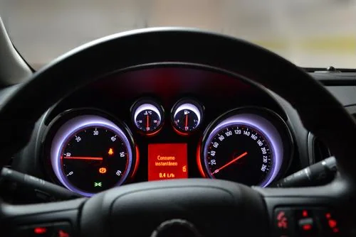
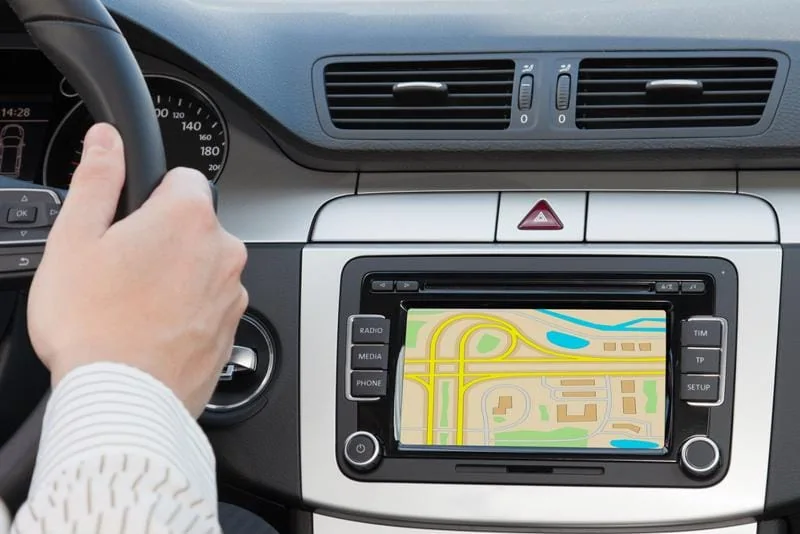
    Electronic and communication technologies are standard features on many automobiles today.
    Electronic and communication technologies are standard features on many automobiles today.

    Why auto manufacturers should work with a photo etching supplier
    For decades, photo etching has been a means by which designers and engineers can solve their trickiest micro problems. With origins in the printed circuit board industry, photo etching has been used in many other sectors like aerospace, electronics, medical and scientific equipment, RF and Microwave and others as a way to create precise flat metal parts.

    Our Comprehensive Guide to Photo Etching answers many designers’ questions.

    Download the Guide

    Auto manufacturers have many of the same needs as these industries, which is why OEMs should consider working with a photo etcher for their component parts. Here are just a few of the benefits that come with working with a photo etching supplier:

    • Parts come free of burrs and deformities. Conventional processes such as stamping or laser cutting can leave burrs, uneven edges and thermal distortions in the final part. Etching is a benign process that doesn’t involve “brute force” or extreme heat, so all parts come free of these distortions.
    • Variety of materials. Auto manufacturers need to make vehicles lighter without decreasing part strength or quality, so they’re experimenting with new materials. We can work with a long list of both common and unusual metals and alloys.
    • Inexpensive tooling. For complex parts at high production volumes, conventional processes often require long lead times and high tooling costs. Photo etching utilizes photo tools, which are stencils of the finished parts that are then etched simultaneously. Phototools generally cost $300 or less and can be generated within a day.
    • Complex designs are simple to producePhotoetching has similarities to a printing process in that the part designs can be immensely intricate without having an impact on the tooling or production process.
    • Tight tolerances. For metal over .005″ thick, we can hold tolerances of +/- 15% of the metal’s thickness. Locational tolerances will be within +/-.001″ of drawing nominal.

    To learn more about how photo etching can help your OEM create precision flat metal parts, call us at 800-443-5218 or email us at sales@conardcorp.com

  4. Photo Etching: 2023’s Top Ten FAQs

    Leave a Comment

    Over the course of a year, we talk with a lot of people–most of whom have questions. We’ve compiled the “frequent fliers” list for you.

    Feel free to reach out to me or Max  should you have questions we didn’t cover here.

    What kinds of material can you etch?

    We can etch a wide variety of metal alloys including many iron, nickel, copper and aluminum alloys, as well as silver and molybdenum. Here’s a list of some of the most popular metals. If you use etched braze foil pre-forms, we can do that, too.

    If you have something in mind, just ask us.

    We don’t etch titanium, tungsten, zirconium, gold and other exotic metals. And we don’t etch anything that is not metal, such as glass or plastic, for example.

    We need to have part and lot numbers etched on our parts. Can you do this?

    No, we don’t do part marking unless we are fabricating the parts at the same time. For part marking, we can recommend tustech.com.

    We’d like to do our own etching in house. Where can we buy a photo etching machine?

    There isn’t a “photo etching machine.” It’s not a photocopier. It takes some serious capital equipment—clean line, laminating, imaging, developing, etching, and stripping machines, 10,000-plus square feet of floor space (minimum), and compliance with a massive-and expensive- amount of local, state and federal environmental regulations. Watch the video here.

    When it comes to etching, let us do it for you. We’ve been doing this since 1965—we’re very good at it.

    We need to have some very fine screens made. What is the smallest hole you can make with photo etching?

    The theoretical minimums would be 100-micron holes on 50-micron material with minimum 125-micron ligament between the holes. Plus or minus about 37 microns. There’s a high probability of missing holes when the process is pushed this far.

    As a rule, the minimum hole size must be at least 110% of metal thickness and minimum center-to-center spacing would be hole diameter plus metal thickness.

    What is the smallest part you can make?

    We’ve made parts as small as .020” diameter. 50,000 pieces fit in a tea cup.

    And, what’s the biggest part?

    We can image up to 27” by 58” sheets.

    What is the range of metal thicknesses that you can etch?

    We have etched stainless steel as thin as .0005”. We routinely etch .001” thick steel, nickel, copper and aluminum alloys. As a practical matter, we prefer to limit thickness on “white metals” (steel, nickel, silver, moly) to a maximum of .040” (~1 mm). The “red metals” (copper, brass, bronze, etc), we will etch up to .065”. And in aluminum, we’ll go up to .080” (~ 2 mm).

     What dimensional tolerances can the etching process achieve?

    Typically, we design the work sheet to achieve average tolerances of +/- 15% of the metal thickness, to a practical minimum of +/-.0015” for metals .010” and less. The size of the work sheet has an impact on both the minimum tolerances and the cost.

    Here’s an example of that relationship.

    Just because your solid modeling environment will let you put extraordinarily tight tolerances on dimensions, doesn’t mean you should. Someone will have to make the part, and no one will want to.

    As we say, “CBYD.” Call before you design.

    Why would I choose photo etching over stamping or laser cutting?

    Here are a few of the advantages offered by photo etching. And, with our recently installed LED-powered direct digital imaging system, we will be able get to production directly from your cad file.

    What about Nadcap? Is photo chemical machining considered to be a “special process?”

    Photo chemical machining is not a Nadcap “special process” because it does not alter the characteristics of the metal. However, chemical milling -as it is often used in aerospace applications- may be subject to Nadcap checklist 7108/5. When chemical milling is used to remove metal from areas of parts selectively, such as engine nacelles, in order to reduce weight, the “characteristic” of the metal thickness has been changed.

  5. Photo Etched Parts are Everywhere, but You Never Knew

    Leave a Comment

    Photo etched metal parts are used in various industrial products across multiple sectors due to their precision, flexibility in design, and cost-effectiveness. Here are some common types of industrial products that use photo etched metal parts:

    1. Electronics

    • Circuit Boards: Photo etching is used to create intricate circuit patterns on metal substrates, commonly found in PCBs (Printed Circuit Boards).
    • EMI/RFI Shields: Shielding components that prevent electromagnetic and radio frequency interference are often made through photo etching.
    • Contacts and Connectors: Electrical connectors and contact points require high precision, which photo etching can achieve.

    2. Automotive

    • Fuel Injector Components: Fine metal parts used in fuel injectors, such as filters, are manufactured using photo etching.
    • Brake and Transmission Components: Precision metal parts within braking systems and transmissions often use photo-etched parts for reliability and durability.
    • Heat Shields: Thin metal components used to protect other parts from heat are often produced using photo etching.

    3. Medical Devices

    • Surgical Instruments: Photo etching is used to manufacture precise and intricate surgical instruments and blades.
    • Medical Implants: Metal parts for medical implants, such as stents, are often produced with photo etching due to the need for extreme accuracy.
    • Filters and Grids: Precision filters used in medical devices to control the flow of liquids or gases.

    4. Aerospace

    • Aircraft Engine Components: Precision parts used in aircraft engines, such as turbine blades and fuel injectors, are manufactured with photo etching.
    • Sensors and Instrumentation: Various sensors and instruments in aircraft rely on finely etched metal parts.
    • Heat Exchangers: Complex metal structures in heat exchangers, used for thermal management, can be made through photo etching.

    5. Telecommunications

    • Antenna Components: Metal parts in antennas and signal transmission devices are often produced using photo etching.
    • Waveguides and Filters: Components that direct and filter signals in telecom equipment are made using photo etching.
    • Connectors and Terminals: Like in electronics, connectors and terminals in telecommunications equipment are often photo-etched.

    6. Consumer Electronics

    • Smartphone Components: Various metal parts in smartphones, such as speaker grilles and battery contacts, are produced using photo etching.
    • Camera Shutters: Precision parts in camera shutters that require exacting tolerances can be made through photo etching.
    • Wearables: Thin, lightweight metal components in wearables like smartwatches are often photo-etched.

    7. Defense

    • Precision Weapons Parts: Components for guided missiles, radar systems, and other precision military equipment are often made with photo etching.
    • Ammunition Components: Parts of munitions that require precision and durability may be manufactured using this method.

    8. Industrial Filtration

    • Fine Mesh Filters: Used in chemical processing, oil refining, and other industries where fine filtration is necessary.
    • Sieve and Screens: Components used for separating particles in various industrial processes.

    9. Micromechanics

    • Watch Components: Intricate gears and other small parts in mechanical watches are often produced using photo etching.
    • Micro Gears and Springs: Tiny mechanical parts used in various precision instruments.

    Photo etching is favored in these industries due to its ability to produce highly detailed parts with fine tolerances, flexibility in design, and the ability to work with a wide range of metals.

    sound-icon
    multipage-icon
    refresh-icon
    dislike-icon
    star-icon
  6. Photo Chemical Etching Subject Matter Expertise Available

    Leave a Comment

    In my experience, professionals involved in designing, engineering, and sourcing precision metal components have a pretty good grasp of a variety of fabrication processes. Except for photo chemical machining (metal etching), to which the response is usually a blank look, shrugged shoulders and a negative head nod. You don’t have to be one of those people any more.

    We really want to make it easy for you to add chemical etching to your portfolio of fabricating knowledge. We’ve put together an assortment of FREE user-friendly resources, including video, whitepapers and blog posts that you can peruse at your convenience.

    3 minutes to greater understanding

    This 3 minute post provides a visual overview of the steps and equipment required for the etching process. Most people have a mental picture of stamping, laser and EDM machinery. Now you can have one for etching.

    The basics on one page

    On this page, we have summarized the key features and capabilities of the photo etching process and have included information on tolerances and costs.

    How else would you do it?

    How does chemical etching stack up compared to stamping, laser and waterjet?  We did a study. You can get the results here.

    DFM matters

    Design-for-manufacture analysis is a critical step in product development. It is particularly important that the people responsible for this process have access to extensive information on the options available. This blog post highlights several key benefits of etching versus other processes.

    It worked for them

    We talk to lots of people about their fabricating challenges, and they are generally astounded when we can tell them that the etching process is a total solution for them. This blog post recounts three instances where etching completely solved the problems.

    Get it all

    We’ve put together a brief (14 pages) but comprehensive guide for chemical etching that covers all of the specs, tolerances, costing examples. It’s FREE. You can get it here:

    Download the Guide

    Answers Available. Questions Wanted.

    You can call me at 860-659-0591. Write me at kstillman@conardcorp.comOr, upload a drawing.

  7. Photo Etching’s role in the booming semiconductor market

    Leave a Comment
    Photo Etching's role in the booming semiconductor market
    Photo Etching has the ability to create complex, precision parts, which will be a boon to semiconductor manufacturers as the Internet of Things gains a bigger foothold in consumer markets.

    Today’s consumer market is witnessing the advent of “smart” products – devices connected to one another over wireless networks, exchanging data between manufacturers and the owners of the products themselves. Common household items are now being manufactured with the capability to join an interconnected network that enables an unprecedented level of communication and data gathering. This trend is colloquially known as the Internet of Things (IoT).

    Smart TVs, automobiles, kitchen appliances, thermostats – all of these and more are poised to replace their unconnected predecessors. A report by the research agency Gartner predicted that 26 billion consumer devices will be taken under the IoT fold by 2020.

    Semiconductor market slated to grow thanks to IoT
    Not only will IoT-connected devices will make a big splash in the consumer goods market, they will also have a major impact on the electronic semiconductor market as well. Government Technology looked at research from Gartner and found that the total size of the semiconductor market is set to grow 30 percent from now until 2020.

    “The demand for billions of things will ripple throughout the entire value chain, from software and services to semiconductor devices,” said Alfonso Velosa, research director at Gartner. “These ‘things’ will drive huge demand for individual chips. IoT semiconductor growth will come from industries spanning consumer, industrial, medical, automotive and others.”

    The hallmark of these products is their ability to communicate through wireless networks. These “things” must be equipped with communication devices without hampering the basic functionality of the product. It’s no surprise, then, that manufacturers want the electronics to be as small as possible without sacrificing output.

    Digital Technologies Rely on Photo Etching
    Smart Watches are just one part of the Internet of Things trend that rely on small but powerful semiconductors for its wireless communication capabilities.

    Photo Etching has a role to play
    Component parts created by Photo Etching are a staple in manufacturing for the RF, Microwave and wireless industries, all of which will be integral in the burgeoning IoT.

    Semiconductors, leadframes and other components in these products often have complex geometries that make them difficult, if not complete impractical to manufacture with other methods such as stamping, laser cutting, etc. This makes Photo Etching a top choice, as it is known for being able to create complicated parts at a low cost and in a short time.

    Another reason why Photo Etching is well-suited for this type of complex production is that we can work with thin-gauge metals and hold tolerances within .001″ in sheets with a thickness of .005″ and under. Additionally, the process produces no burrs or thermal distortions in the finished product.

    In terms of materials, copper alloys like brass and beryllium copper are two metals frequently used in making component parts for wireless applications. We are well versed in working with these and other metals, having honed the etching process for this type of work over the last 49 years we’ve been in business.

    If you’re an OEM in the semiconductor space, call us at 800-443-5218 or email us at sales@conardcorp.com and we can get started working on your designs!

    Download Now
    Engineering Design
    Guidelines

  8. Photo Etching Is Cost-Effective For Production Quantities

    Leave a Comment
    Photo Etching Is Cost-Effective For Production Quantities
    Photo etching is a cost-effective fabrication method, regardless of production volume or part complexity.

    Engineers and designers use several criteria to evaluate their options for fabrication methods, and one of the most important is the value they get for the production volume they need. Some methods, like laser cutting and stamping, are cost-effective for simple parts at low to high volumes. But the problem with those processes is that as the desired part’s geometric complexity increases, their tooling, set up and material costs all rise dramatically.

    Photo etching is well-suited to handling odd shapes and miniscule surface features at volumes ranging from dozens to tens of thousands. Best of all, the production costs of the parts don’t spiral out of control just because the amount of parts needed increases. Our ability to deliver value to our customers regardless of the quantities they need us to produce starts with our “tools.”

    “The phototool is a fast, flexible and inexpensive way to produce an array of precision flat metal parts.”

    The phototool’s role in cost-effective production
    The phototool is a fast, flexible and inexpensive way to produce an array of precision flat metal parts when compared to dies or steel tools. Once we have a CAD file of the design, we can generate a phototool in a matter of hours and for around $300 or less. Other fabrication methods have lead times ranging from weeks to months. Finally, if you have design changes, the phototools can be easily regenerated to accommodate revisions without incurring substantial costs or wasted time making new tools.

    A phototool is a stencil of the finished part printed on dimensionally stable mylar using an 8,000-dpi photoplotter. Since UV light is the phototool’s only working exposure, there is no tool wear in the traditional sense of a die or drill getting worn out from multiple uses. This means that we don’t have to keep replacing our tools or worry about tool wear leading to uneven dimensions that are out of tolerance.

    Saving money on precision metal part production starts with the phototool.
    Saving money on precision metal part production starts with the phototool.

    Photo etching handles complexity well, even at high production volumes
    Phototools lend themselves to rapid and cost-effective production regardless of the part’s geometry – whether we need to make 10 or 10,000 parts. Very often, we’re asked to make parts with hundreds of tiny holes on the surface, and this complexity is where etching excels.

    As a matter of comparison, both stamping and etching can produce hundreds of holes simultaneously, but punching requires multiple strikes and the linear processes – laser, plasma and wire EDM – must make each hole one at a time. The more holes required, the more expensive the stamping dies become. With a phototool, whether it’s one hole or 1,000, the cost of the tool doesn’t change and is typically less than $300.

    For more intricate parts like small grids or leadframes, the difference between etching and the other processes is even more pronounced. The Photo Chemical Machining Institute asked manufacturers using a variety of process to quote them a price for a .005″ stainless steel or nickel grid with a diameter of 1″. The stamper, EDM and water jet cutter all said that the parts were too intricate and impractical to make in any batch size. The laser cutter was the only one that could do it, but at about 300% of the tooling and set up costs a photo etcher would charge for a batch of 5,000 parts. Photo etching, on the other hand, could handle the complexity and a variety of batch sizes ranging from 100 to 50,000 without subjecting the customer to burdensome cost increases.

    For more information, download the Comprehesive Guide to Photo Etching:

    Get The Guide Now

    To learn more about how your OEM can benefit from working with a photo etcher, regardless of your production quantity needs, call us at 800-443-5218 or email us at sales@conardcorp.com.

  9. Photo Etching for Metal Stampers: another way to say ‘yes’

    Leave a Comment
    Photo Etching for Metal Stampers: another way to say 'yes'
    Many stampers have found that working with a photo etcher can help them meet a wider array of their customer’s needs and enable them to say, “Yes, we can do that for you.”

    No one likes to say no to a customer. But sometimes, your customer’s’ requests are just not a good fit for your processes. For metal stampers, you may find that the gap between what you want and what you can do in reality is a bit wider than you think with certain designs.

    The following issues are some of the common that metal stampers run into:

    • High tooling costs.
    • Long lead and production times.
    • Production methods can’t accommodate design complexity.
    • The desired material/thickness combination is not possible.
    • Dimensional tolerances are too tight.
    • The customer wants too low a quantity.

    Photo etching can set metal stampers on the path to saying “yes!”
    Many stampers have found that working with a photo etcher can help them meet a wider array of their customer’s needs and enable them to say, “Yes, we can do that for you.” Here is how working with a photo etching supplier can address the common problems listed above.

    • Photo tools can be made in 24 hours and are usually less than $300.
    • Prototyped quantities can be produced within days.
    • Nearly any quantity is acceptable – from tens to thousands.
    • Suitable for materials as thin as .001″.
    • Accommodate tight tolerances, +/- 15% of metal thickness.
    • Design complexity is a non-issue.

    “Design complexity is a non-issue.”

    For many industries today, tight tolerances, small parts and complex designs are becoming the norm for component parts. The MEMS, medical and the RF industries are just a few that are asking suppliers to make their parts even smaller and more precise. If metal stampers want to stay competitive, they must find a way to adapt to these changes. Working with a photo etcher help them expand their palette of offerings to their customers.

    Photo Etched Medical Sensors
    Complex component parts are a growing part of the medical equipment industry. Photo etching can help metal stampers say yes to their customers in this growing field.

    How metal stamping compares to photo etching for complex parts
    To get an idea of how other nonconventional fabrication methods stack up against photo etching when producing complex flat parts, the Photo Chemical Machining Institute asked a variety of suppliers to quote prices for some common yet complicated parts.

    The PCMI found that as parts call for more complex design features and geometries, metal stamping becomes far less cost efficient. For example, a typical leadframe used in electronic applications wouldn’t be practical in any batch size smaller than 50,000. For a batch size of 50,000 leadframes, stamping’s tooling costs turned out to be 20,000 percent compared to those of a photoetcher.

    For a grid that would find its home in the medical equipment industry, stamping turned out to be completely impractical – the supplier who quoted the price said that no batch size for the part would ever be feasible for stamping. The tolerances for the grid’s aperture are simply too tight for stamping to produce them to the design’s specifications.

    If you’re a metal stamper who has a customer requesting a job outside your area of expertise, call us at 800-443-5218 or email us at sales@conardcorp.com so we can help you say “yes”!

    Request a Quote

  10. High Complexity Designs Made Easier by Photo Etching

    Leave a Comment
    Photo etching: A powerful option for complex precision products
    Photo etching enables the creation of complex precision parts while keeping production times and costs low.

    Engineers and designers at OEMs are often tasked with creating startlingly complex parts while keeping costs and time to market down to a minimum.

    For fabricating simple product geometries, photo etching is certainly a smart choice, but the difference between it and other methods may not be as pronounced. However, as these designs become more complex, photo etching’s unique advantages offer substantial benefits in cost and precision.

    Why does photo etching lend itself so well to complex applications?
    Photo etching has proven to be superior to other methods both conventional and nonconventional when it comes to producing complicated products with a high degree of precision.

    In photo etching, the part is machined all at once because the process etches through all unmasked areas of the plate simultaneously. Other methods like CNC punching, laser cutting and wire EDMs work on a small, localized area of the part at one time. These methods take more time than photo etching, are highly vulnerable to undesirable effects like tool wear, uneven locational tolerances and thermal and/or mechanical distortions that lead to deficiencies in the final product.

    OEMs take notice of photo etching’s capabilities
    Dr. David M. Allen, a professor of micro engineering at Cranfield University in England, wrote that photo etching has drawn the eyes of engineers and designers in the microelectronics, mechanical and electrical industries over the last half-century for its ability to provide quick response service for complex precision parts.

    OEMs in these verticals have a high demand for thin gauge (< 2mm in thickness) precision component parts of varying complexity at as low a price point as possible. Allen found that some of the most common examples of this are integrated circuit leadframes, disk drive suspension head assemblies, sieves and meshes, washers, laminations and etched gaskets for use in mobile phones.

    Lead frames – a point of comparison between fabrication methods
    To test specific examples of photo etching’s capacity to deal with complex geometries, the Photo Chemical Machining Institute (PCMI) asked a wide range of companies proficient in different production methods to quote them for parts of various intricacy. Based on the quotes obtained, it was apparent that photo etching was the superior fabrication method as part complexity increased.

    One part for which the PCMI received a quote is a lead frame – a part commonly used in electronic circuits. The organization asked a variety of manufacturers to quote them for a 1 inch lead frame made of nickel iron with a thickness of .008″ and a dimensional tolerance of +/- .001″.

    The only method that found it practical to even attempt to make leadframes was laser cutting. The quoted price for tooling and setup for the laser cutting of 100 parts was 270 percent of the price that photo etching could do for the same part. For bulk purchases, it turned out that the cost of manufacturing 5,000 leadframes was also 270 percent of the cost of etching the same size batch. Batches of 50,000 and above were found to be impractical for laser cutters.

    Other fabrication methods like stamping, wire EDM and water jet cutting fared even worse. These companies couldn’t even quote a price for lead frame manufacture – they all found it to be impractical even in small batches due to the complexity of the part.

    Engineers and designers have many options for simple precision parts. But for the more complex products, the capabilities of photo etching can keep production times and costs low.

    Request a Quote