Exit

Author Archives: Conard Corporation.

  1. Photo Etching is All Around Us

    Leave a Comment

    What is Photo Chemical Machining?

    Before diving into its applications, it’s important to briefly understand the PCM process. PCM involves coating a metal sheet with a photoresist, which is then exposed to UV light through a photomask with the desired design. The exposed areas act as a stencil to protect parts of the metal during the chemical etching stage. Once etched, the metal is left with intricate and accurate designs.

    This process is ideal for creating parts with fine details, high precision, and tight tolerances, which are critical in industries like electronics, aerospace, medical devices, and automotive. However, despite its technological significance, PCM’s contributions are rarely appreciated in the context of everyday products.

    PCM and Electronics: Hidden in Plain Sight

    One of the most significant, yet often overlooked, roles of PCM is in the production of consumer electronics. The complex circuits, connectors, and metal components inside smartphones, laptops, cameras, and tablets are often produced using PCM.

    Take, for example, the printed circuit boards (PCBs) that power our electronics. PCM is employed to create the intricate pathways through which electrical signals pass, enabling devices to function efficiently. PCM’s high level of precision allows for the creation of these delicate, miniature parts with the accuracy required to handle the growing complexity of modern electronics. Without PCM, it would be far more challenging to mass-produce these components at a cost-effective rate, especially considering the ever-decreasing size of devices.

    Moreover, the metallic mesh components used in smartphone microphones, speakers, and sensors are frequently produced using PCM. These tiny parts, often smaller than a grain of rice, are critical to the functionality of the devices we use every day, and yet, they remain hidden from our awareness.

    PCM in Automotive and Aerospace: Safety and Efficiency

    The automotive industry is another area where PCM’s contributions are largely overlooked. PCM is commonly used to produce precision metal parts such as fuel injector nozzles, filters, and various sensors that contribute to the performance and safety of vehicles. Fuel injectors, for example, must deliver fuel in precise amounts and at high pressures to ensure the engine operates efficiently. PCM enables the production of injector nozzles with tiny, consistent apertures that provide this precision.

    Furthermore, PCM plays a role in the aerospace industry, where lightweight, durable components are critical to flight safety and fuel efficiency. While these applications are critical for safe and efficient air travel, the everyday traveler rarely considers how PCM helps keep planes in the sky and vehicles on the road.

    Medical Devices: Precision That Saves Lives

    PCM’s contributions to medical devices may be one of the most vital areas of its impact. Surgical instruments, pacemakers, stents, and a variety of analytical and diagnostic devices often feature parts produced using PCM.

    For example, the stents used to open up arteries in cardiovascular treatments require precise dimensions to ensure proper blood flow. PCM allows manufacturers to produce these life-saving devices with the exacting precision necessary for use in delicate medical procedures.

    Check Out Your Own Home

    Your own kitchen could be a hot bed of photo etched products:

    • French press and pour-over coffee filters
    • Vegetable peelers and “zoodle” makers
    • Cheese graters
    • Fruit and nut zesters
    • Spice and herb mills

    And in the bathroom:

    • Electric shaver foils
    • Pedicure and callus files

    And the workshop:

    • Hacksaw and other saw blades
    • Planes

    The Future of PCM in Everyday Products

    As technology continues to evolve, the role of PCM in everyday products will only grow. With advancements in miniaturization, especially in fields like electronics and medical devices, the demand for highly precise, intricate components will continue to rise. PCM’s unique ability to produce such parts at scale and with unmatched precision ensures that it will remain a key manufacturing process.

    However, despite its vital role, PCM remains largely underappreciated. Most consumers remain unaware of how integral this technology is to the functionality of the products they use every day. By understanding the widespread applications of PCM—from smartphones and automobiles to medical devices—we can gain a greater appreciation for this silent, yet indispensable, process.

  2. 5 Reasons to Choose Photo-Etched Pre-forms for Brazing Applications

    Leave a Comment

    Photo etched braze foil pre-forms offer numerous benefits over traditional braze and filler pastes or powders when used in vacuum and dip brazing applications in the aerospace industry. Aerospace components demand high precision, strength, and reliability, which makes the choice of brazing materials and techniques crucial. The advantages of using photo etched braze foil pre-forms include improved precision, superior joint integrity, increased manufacturing efficiency, reduced waste, and enhanced cleanliness, all of which contribute to higher-quality assemblies.

    1. Enhanced Precision and Consistency

    One of the primary benefits of photo etched braze foil pre-forms is the superior precision they offer in terms of shape, thickness, and weight. Photo etching allows for the production of complex, highly accurate patterns tailored to the exact geometrical requirements of the components being brazed. Unlike pastes and powders that require manual application, foil pre-forms are pre-cut to fit the joint precisely, ensuring uniform distribution of braze material. This precision reduces the risk of joint voids, uneven bonding, or excess material that could compromise component integrity.

    The uniformity of thickness in pre-forms also eliminates variations in the amount of braze material applied, leading to consistent capillary action during brazing. This consistency improves the predictability and repeatability of brazed joints, which is critical in aerospace applications where uniform performance and reliability are non-negotiable.

    2. Superior Joint Integrity

    Braze foil pre-forms contribute to superior joint strength and reliability. In vacuum and dip brazing, achieving a solid, uniform bond between components is essential. The uniform composition and controlled thickness of photo etched foil allow for even melting and distribution of the braze alloy, resulting in joints that exhibit higher mechanical strength and fewer defects than those formed using pastes or powders.

    Pastes and powders may contain binders and additives that can introduce contaminants or leave residues after brazing. In contrast, pre-forms are typically free of these additives, reducing the risk of contamination and improving the metallurgical integrity of the joint. This is particularly important in aerospace applications, where joints are subjected to extreme thermal, mechanical, and environmental stresses.

    3. Improved Manufacturing Efficiency

    Using photo etched braze foil pre-forms streamlines the manufacturing process, reducing preparation and assembly time. Since pre-forms are custom-cut to fit specific joint geometries, they minimize the need for manual shaping, trimming, or repositioning. This pre-fabrication reduces assembly errors and speeds up production, making the process more efficient and less labor-intensive.

    In contrast, pastes and powders require precise manual application, which can be time-consuming and prone to variability. Additionally, paste application often involves multiple steps, including drying and binder removal, adding to the overall process time. Pre-forms eliminate these extra steps, reducing cycle times and enhancing throughput.

    4. Reduced Waste and Material Cost Savings

    Pre-forms are manufactured to exact specifications, meaning they provide only the necessary amount of braze alloy required for a given joint. This precision significantly reduces material waste compared to pastes and powders, where excess material can be inadvertently applied or lost during handling. The reduction in waste leads to cost savings, especially when working with expensive brazing alloys commonly used in aerospace applications, such as nickel-based or silver-based alloys.

    Moreover, the minimized need for rework or scrap caused by uneven joints or excess filler material further enhances cost-effectiveness and resource efficiency.

    5. Enhanced Cleanliness and Process Control

    In aerospace manufacturing, cleanliness is a critical factor due to the sensitivity of components to contamination. Photo etched braze foil pre-forms do not require binders, fluxes, or other additives that are often present in pastes and powders. This characteristic makes them ideal for vacuum brazing, where a high-purity, controlled atmosphere is required to prevent oxidation and ensure optimal bonding.

    The absence of binders also eliminates issues related to off-gassing or residue formation, which can degrade joint quality. Additionally, pre-forms facilitate better process control by providing consistent, pre-measured amounts of brazing material, reducing variability and enhancing quality assurance.

    Conclusion

    Photo etched braze foil pre-forms offer significant advantages over traditional pastes and powders for vacuum and dip brazing in aerospace applications. They provide enhanced precision, superior joint integrity, improved manufacturing efficiency, reduced waste, and a cleaner brazing process. These benefits contribute to higher quality, more reliable aerospace components, making photo etched pre-forms an indispensable choice for critical brazing applications.

  3. What to Know About 3 Key Variables in Etching

    Leave a Comment

    Here’s a detailed explanation of how etching solution temperature, spray bar pressure, and oxidation-reduction potential (ORP) influence accuracy and consistency in photo chemical machining (PCM):


    Impact of Etching Solution Temperature

    The temperature of the etching solution plays a critical role in determining the rate and uniformity of material removal in PCM. The etching process relies on chemical reactions between the etchant (such as ferric chloride) and the metal surface. These reactions are temperature-dependent, meaning that:

    1. Higher Temperatures Increase Etch Rate

      • Elevated temperatures enhance the kinetic energy of the reactant molecules, accelerating the chemical dissolution of metal.
      • While this speeds up processing times, excessive temperatures can lead to over-etching, loss of precision, and undercutting (where etchant removes material under the photoresist mask).
    2. Lower Temperatures Slow the Process

      • Insufficient temperatures reduce the reaction rate, leading to incomplete etching and longer processing times.
      • Inconsistent temperature distribution within the etching bath can cause variations in etch depth, affecting accuracy and repeatability.
    3. Maintaining Optimal Temperature

      • Most industrial PCM operations maintain etching solutions between 45°C and 55°C to balance speed and accuracy.
      • Temperature control systems, such as immersion heaters and recirculating cooling systems, help ensure uniformity.

    Effect of Spray Bar Pressure on Accuracy and Consistency

    The spray bar delivers the etchant to the workpiece, ensuring uniform distribution and efficient material removal. The pressure of the spray directly impacts how the etchant interacts with the metal surface.

    1. High Spray Pressure Enhances Uniformity

      • Higher pressure improves solution flow dynamics, reducing stagnant areas where etching could be uneven.
      • Ensures fresh etchant reaches the workpiece continuously, preventing localized depletion of active chemicals.
      • However, excessive pressure can cause splashing and turbulence, leading to uneven etching.
    2. Low Spray Pressure Leads to Inconsistencies

      • Inadequate pressure results in poor circulation, allowing reaction byproducts to accumulate and slow down etching.
      • This can lead to differential etch rates across the workpiece, causing variations in feature dimensions.
    3. Optimizing Spray Pressure

      • Typical pressures range from 1.5 to 3.5 bar, depending on the metal thickness and feature resolution.
      • Adjustable nozzles and strategically placed spray bars improve etching efficiency and minimize undercutting.

    Influence of Oxidation-Reduction Potential (ORP) on Process Stability

    Oxidation-reduction potential (ORP) is a measure of the chemical activity of the etching solution, specifically its ability to oxidize and dissolve metal effectively. ORP is crucial for process consistency and accuracy.

    1. High ORP Indicates Strong Etching Action

      • ORP values above the optimal range may lead to aggressive etching, increasing the risk of excessive material removal and loss of fine features.
      • Oxidation byproducts, such as metal salts, can accumulate and reduce etching efficiency over time.
    2. Low ORP Reduces Etching Effectiveness

      • If ORP drops too low, the etchant loses its ability to dissolve metal efficiently, leading to incomplete etching.
      • This can cause uneven feature definition, requiring rework or resulting in defective parts.
    3. Maintaining ORP for Consistency

      • ORP is typically maintained in the range of 450–650 mV for ferric chloride solutions.
      • Regular monitoring and chemical replenishment (e.g., adding oxidizing agents like hydrogen peroxide) help sustain the optimal ORP level.

    Conclusion

    In photo chemical machining, etching solution temperature, spray bar pressure, and ORP must be carefully controlled to ensure accurate and consistent results. A stable temperature optimizes the reaction rate, appropriate spray pressure enhances uniformity, and proper ORP management maintains chemical effectiveness. By fine-tuning these parameters, manufacturers can achieve high precision and repeatability in producing complex metal components.

  4. Design for Manufacturability (DFM) in Photo Chemical Machining: A Guide for Engineers and Designers

    Leave a Comment

    In the world of precision metal components, achieving intricate designs with tight tolerances can be a challenge. Photo Chemical Machining (PCM) offers a unique manufacturing process that eliminates mechanical stress, enabling the production of complex parts with high precision. However, to maximize the benefits of PCM, engineers and designers must apply Design for Manufacturability (DFM) principles.

    DFM helps ensure that parts are not only functional but also optimized for efficient, cost-effective production. By integrating DFM into your design process, you can reduce manufacturing costs, improve quality, and accelerate time to market.

    What Is Photo Chemical Machining?

    PCM, also known as chemical etching, is a subtractive manufacturing process that uses photolithography and chemical etching to remove material from thin metal sheets. It is ideal for producing intricate parts with fine features, tight tolerances, and complex geometries that would be difficult or expensive to achieve with traditional machining methods like stamping, laser cutting, or CNC milling.

    PCM offers several advantages, including:

    • No mechanical stress or heat-affected zones
    • Burr-free and distortion-free parts
    • Design flexibility with fine detail capabilities
    • Fast prototyping and scalable production

    However, like any manufacturing process, PCM has its own design constraints. Applying DFM principles ensures that your parts are optimized for etching, reducing waste and minimizing production challenges.

    DFM Considerations for PCM

    1. Material Selection

    PCM works with a wide range of metals, including:

    • Stainless steel (for corrosion resistance and strength)
    • Copper and brass (for electrical conductivity)
    • Nickel alloys (for high-temperature applications)

    Choosing the right material early in the design process ensures compatibility with etching chemistry and maintains desired mechanical properties.

    1. Feature Design & Etch Factor

    Unlike mechanical machining, PCM etches isotropically, meaning material is removed uniformly in all directions. This results in an etch factor, where the width of an etched feature is affected by the depth of material removal. A typical guideline is:

    • Minimum feature size = metal thickness
    • Hole diameters should be at least 1.1x material thickness
    • Slots and fine features should be designed with gradual transitions to avoid over-etching

    By accounting for the etch factor, designers can ensure features remain precise and manufacturable.

    1. Tolerances & Undercut Control

    PCM can achieve tolerances of ±10% of the metal thickness, but this varies based on material type and feature complexity. It can also have a significant impact on cost. You may think that tighter tolerances mean a “better” part, but you should ask about reduicng costs by opening tolerances. It might surprise you.

    • Critical features should have relaxed tolerances when possible to simplify production.
    • Undercut occurs when chemical etching removes material beneath the resist mask. Designing with undercut compensation—such as widening narrow features—helps maintain accuracy.
    1. Masking & Etching Strategy

    PCM uses photoresist masking to define which areas will be etched. Proper design considerations include:

    • Double-sided etching allows for complex geometries but requires alignment precision.
    • Partial etching (step etching) can create variable thickness features but should be designed carefully to avoid over-etching.
    • Tab placement can prevent part distortion during etching and handling.
    1. Cost & Efficiency Optimization

    Applying DFM principles can lead to significant cost savings. Considerations include:

    • Nesting multiple parts in a single sheet to maximize material usage.
    • Reducing unnecessary fine details that increase etching time and complexity.
    • Avoiding deep etches when possible to minimize process variations.

    Early collaboration with a PCM specialist ensures your design is optimized for manufacturability before production begins.

    Conclusion

    Photo Chemical Machining is a powerful process for precision metal components, but achieving optimal results requires careful DFM considerations. By designing with etch factor, material properties, feature tolerances, and process limitations in mind, engineers and designers can create parts that are not only functional but also cost-effective and manufacturable at scale.

    Are you working on a project that could benefit from PCM? Contact our team of experts to discuss how DFM can enhance your designs!

  5. When PCM is a Superior Option to Stamping, Laser Cutting, or Wire EDM

    Leave a Comment

    When Photo Chemical Machining is Superior to Stamping, Laser Cutting, and Wire EDM

    Photo Chemical Machining (PCM), also known as photo etching, is a highly precise, versatile metal fabrication process that offers significant advantages over traditional manufacturing methods like stamping, laser cutting, and wire Electrical Discharge Machining (EDM). While each of these techniques has its place in metal fabrication, PCM excels in applications that demand intricate designs, stress-free parts, fine detail, and cost-effective prototyping or low-to-medium volume production. Here are some specific applications where PCM provides a superior solution.

    1. Aerospace and Aviation Components

    Aerospace parts often require extreme precision, lightweight materials, and complex geometries. PCM is ideal for fabricating thin, intricate metal components like:

    • Turbine engine cooling plates – PCM produces these with fine perforations and intricate channels without introducing stress or heat-affected zones (HAZ), which could compromise performance.
    • EMI/RFI shielding for avionics – The process allows the creation of custom shielding with complex patterns in lightweight materials without compromising conductivity or mechanical integrity.
    • Fuel and fluid filtration screens – PCM allows for precise, burr-free micro-perforations that optimize fluid flow without requiring secondary finishing.

    Unlike stamping, which can cause warping or stress fractures in delicate aerospace parts, PCM provides a distortion-free method that preserves the mechanical properties of materials like Inconel and other high-nickel alloys, which are commonly used in aerospace applications.

    1. Medical Device Manufacturing

    The medical industry demands high precision, biocompatibility, and complex micro-scale designs for devices such as:

    • Surgical blades and saws – PCM allows for the production of ultra-sharp, burr-free cutting edges that are essential for surgical precision.
    • Implantable components and stents – Unlike stamping, which can cause stress-induced microcracks, PCM produces intricate stents and implantable structures without affecting material properties.
    • Microfluidic devices – PCM can create precise channels and filters for lab-on-chip diagnostic devices, ensuring smooth fluid flow without rough edges.

    Compared to laser cutting or EDM, which may introduce heat-induced material changes, PCM ensures that the original material properties remain unchanged, making it ideal for medical-grade stainless steels.

    1. Precision Electronics and Semiconductor Components

    PCM is widely used in the production of electronic and semiconductor components, where precision and fine feature control are paramount. Key applications include:

    • Lead frames and connectors – PCM allows for tight tolerances and complex geometries that would be challenging or expensive to produce with stamping.
    • Heat sinks and thermal management components – The process enables the production of intricate cooling structures with optimal thermal efficiency.
    • Flexible circuit boards and thin metal interconnects – PCM produces thin, highly precise features without mechanical stress, preventing damage to delicate circuitry.

    Unlike wire EDM, which is limited by the need for an electrical connection to the workpiece, PCM can process non-conductive coatings on conductive materials, expanding design possibilities for hybrid electronic applications.

    1. Automotive and Fuel System Components

    In the automotive industry, PCM is preferred for manufacturing lightweight, high-precision components such as:

    • Fuel injection nozzles – PCM creates highly accurate micro-holes for fuel atomization, enhancing engine efficiency.
    • EV battery cooling plates and heat exchangers – PCM enables the production of intricate cooling channel designs that are essential for optimal battery performance.
    • EMI shielding for automotive electronics – As vehicles become more reliant on electronics, PCM provides a fast and precise method for manufacturing shielding components.

    Stamping can create deformation in thin metal sheets, affecting fuel injector performance, while laser cutting may introduce unwanted heat effects. PCM eliminates both of these issues, providing burr-free and stress-free parts.

    1. RF and Microwave Communication Systems

    PCM is a go-to solution for high-frequency communication components, where precise tolerances and intricate patterns are required, such as:

    • Waveguides and antennas – PCM allows for the manufacturing of lightweight, precisely tuned components for optimal signal transmission.
    • Microwave filters and resonators – The ability to etch precise slot patterns and cavity structures makes PCM ideal for RF applications.

    Unlike stamping, which can create inconsistencies in metal thickness and introduce stresses, PCM ensures uniformity and precision that is critical for radiofrequency performance.

    1. Specialty and Custom Prototyping Applications

    For industries requiring rapid prototyping and low-volume production of complex parts, PCM is a cost-effective solution. Applications include:

    • Custom aerospace and defense components – Rapid prototyping of intricate structures without the need for expensive tooling.
    • Scientific instrumentation – Custom precision components for optics, research equipment, and experimental setups.

    Unlike stamping, which requires expensive tooling changes, or laser cutting, which may leave heat-affected edges requiring post-processing, PCM provides a more efficient and cost-effective approach for custom, low-volume parts.

    Conclusion

    Photo Chemical Machining stands out as a superior fabrication method in applications requiring intricate detailing, stress-free processing, high precision, and cost-effective prototyping. It offers clear advantages over stamping (which can deform or stress metal), laser cutting (which introduces heat-affected zones), and wire EDM (which is slower and limited in material versatility). Industries such as aerospace, medical, electronics, automotive, RF communication, and custom prototyping all benefit from PCM’s unique ability to create high-quality, burr-free, and precisely detailed metal components.

  6. Why We Love Photo Etching and You should too!

    Leave a Comment
    Why We Love Photo Etching and You should too!

    Photo etching may not have the glamour and sparkle of laser and plasma cutting or the brute force sturm und drang of stamping or punching, but it does have a certain elegance and finesse. It has a deceptive gentleness…after all, we are simply washing away the unneeded metal with equipment that would remind you more of a commercial dishwasher than a machine tool.

    The versatility of photo etching finds applications in a broad swath of industries. We have discussed its use in producing leadframes, lids and contacts for microelectronics packaging. There are a host of industrial products that make use of etched components including batteries, bearings, belts, motors, filtration, sensors and gauges…and on and on.

    Precision etched components also find their way into an impressive array of medical, scientific, environmental and industrial instrumentation and control systems. Aerospace and defense technologies make use of  etched metal parts in a wide variety of ways, as well.

    That’s part of what we love about photo etching….there are so many ways it can be used. And yes, of course, it is very popular for jewelry, ornaments, model making and an extensive assortment of premium giftware.

    Chemical machining (just another name for it) is especially well suited to working with very thin metals, down to .0005″ thick (really, though we don’t recommend it…very expensive). The sweet spot for the process is .032″ and under. We will etch copper alloys up to .065″ thick and aluminum up to .080″ thick.

    And, that’s another thing to remember. We love to etch aluminum. Most etchers don’t. That’s because we have a process for aluminum that was developed by a metallurgist and is the best in the industry. So, don’t be afraid of etching aluminum… we’re not.

    Making holes is another thing to love about chemical machining. One hole, a million holes..it’s all the same to us. Big holes, little holes (down to .004″!), any shaped holes. Photo etching does a fabulous job and cheap, too!

    Complex shapes are easy. Tooling is cheap and quick (generally under $300 and 2 days.) Little parts (as small as .020″ diameter, big parts (up to 24″ x 60″) and practically anything in between. If you can draw it, we can probably make it.

    We want to make it easy for you to love the process, too. There are a few design rules you should know, and some cost factors that you may find helpful.

    But, you don’t have to do all the work. We would be happy to provide an Instant Estimate.

    Feel free to contact us with any questions you may have!

    Submit a Technical Question

  7. Why Use Photo Etching for Power Electronic Devices

    Leave a Comment

    The umbrella term “power electronics” refers to a range of semiconductor devices that are used to manage and manipulate the voltage, current and frequency of electric power.

    Why Use Photo Etching for Power Electronic Devices
    • If it has a battery, it needs a special semiconductor that maintains the correct operating voltage to the device regardless of the voltage state of the battery.
    • If it plugs into the wall, it needs a device to convert and step down the AC to DC.
    • If you are charging a battery from an AC source, you need a semiconductor that converts the AC to DC at the correct voltage.
    • If you are generating electricity from a variable source such as wind, solar, hydro, you need a semiconductor that converts the fluctuating AC to “clean” DC and then back to “clean” AC.
    • Uninterruptible power supplies store DC power and output AC power.

    Common names for these types of devices include inverters, converters, and rectifiers. It’s all about managing and converting flows of alternating (AC) and direct (DC) current.

    And, whenever you are dealing with the flow of electric current, you are also dealing with heat. Delicate electronics and heat are not a good combination.

    The modern solution is to combine a conductive material, like copper, with a non-conductive material that is also good at dissipating heat. That’’s where ceramics come in handy. They don’’t conduct electricity and they are good at dissipating heat.

    Direct bond copper (DBC) is the go-to solution. Copper foil, usually 5-, 8- or 12-mils thick is diffusion bonded to one or both sides of a ceramic card.

    The most widely used ceramic is aluminum oxide, or alumina, which has heat dissipating capacity up to about 48 w/mK (watts per meter*Kelvin.)  Aluminum nitride (AlN) can dissipate over 150 w/mK. Aluminum nitride is about 3 times the cost of alumina.

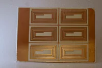
    Fabricating the DBC substrates into useful devices relies on photo etching the circuits into the copper. Chemical etching selectively removes the copper without affecting the ceramic in any way. The phototool is designed to replicate as many copies of the DBC circuit as will fit on the tile. The individual circuits are spaced to allow secondary fabricating processes after photo etching.

    Additional fabricating steps include laser scribing and, often, hole drilling. The laser scribing allows the ceramic to be cleanly snapped into single circuits. Most often, the etched substrates are plated with electroless nickel and immersion gold, a process known as ENIG. Given the current cost of gold, some users are switching to a three step plating process known as ENEPIG, which places a layer of electroless palladium under the gold to allow the gold weight to be reduced.

    The etched, scribed and plated substrates typically will have one or more surface mounted components wire bonded to the gold. After the components are assembled, the individual circuits are singulated and are ready for the next assembly process.

    DBC circuits are found in nearly every mobile device and a wide range of wireless communications products. As devices become smaller and more powerful, the need for DBC circuits to manage energy and heat becomes ever more important.

    Photo chemical etching is the most cost effective solution for processing copper on ceramic substrates. It produces a crisp, clean circuit free of burrs or distortions. We have extensive experience etching clad substrates products for a wide variety of applications.

    If you would like more information, please:

    Request Info on DBC

  8. Why Use Photo Etching for Aerospace Applications

    Leave a Comment

    Modern aircraft are making use of very high-tech materials, including carbon fiber and advanced composites, for many elements of airframes. But not all elements can be replaced with non-metallic materials. When it has to be metal, aluminum is most often the metal of choice.

    Why?  Because, all other things being equal, an aluminum part will be about one-third the weight of the same part in steel, copper or brass. And, weight matters in any type of air- or space craft.

    As a point of reference, the 747 is about 80% aluminum, the 777 about 70%, and the 787 is 50% aluminum. Although advanced materials are displacing a fair amount of metal, aluminum is still the predominant alloy in use. Titanium is only about 63% heavier, but it is much more expensive and more difficult to fabricate.

    E009

    Aluminum is readily fabricated by many conventional methods. including casting, extruding, forging, machining, punching, stamping, and so forth. It is less compatible with non-conventional processes, such as plasma, laser and wire EDM due to its comparatively low melting point (1220 deg F). It also has very high reflectance (92% of visible light and up to 98% of infrared) which poses issues for many lasers.

    Photochemical machining (or etching) is a non-conventional process that completely avoids the problems of heat and reflectance. The etching process runs at about 135 deg F and has no optical properties. This isn’t to say that etching aluminum is not without challenges. It oxidizes readily and is exothermic. At 536 deg F, it will oxidize in water, producing hydrogen, aluminum hydroxide and (a lot of) heat.

    Controlling the aluminum etching process started with a metallurgist’s deep understanding of the properties and behavior of the alloy. This led to the development of specialized etching solutions and process controls that keep the reaction in check and produce precision components that are smut-free and have smooth, consistent sidewalls.

    Photo etching is suitable for aluminum up to .080″ thick. With the growing deployment of In-Flight WiFi, the need for lightweight, high-bandwidth antenna systems is increasing rapidly. Chemical etching has long been a go-to solution for designers of terrestrial systems, using mostly copper and brass components. Antenna designs rendered in aluminum are just as readily produced.

    Aluminum’s thermal conductivity is important in managing heat dissipation in avionics bays. Photo etching can produce partial etch surface features (at no additional time or cost) that can increase the effective surface area of a low profile heatsink by 25% or more.

    Etched metal parts in a variety of alloys are found in many different subsystems of aircraft:  fuel control systems, hydraulic systems, de-icing boots on prop planes, Faraday grids in aircraft windows, and many more.

    Designers of aerospace components should consider chemical etching as a key fabrication method, particularly for parts with unusual geometries. The costs of the etching process are driven by the “real estate;” the length, width and thickness of the part, not by the complexity. Even for screens or grids, the number of holes has no bearing on the cost of the parts, the cycle time or the costs of the tooling (which is typically less than $300 and available in a day.)

    The etching process can produce metal parts as small as .020″ diameter and up to 24″ x 60″.

    The Comprehensive Guide to Photochemical Machining brings together the information about

    The Guide is free and you can get it here:

    Download the Guide
  9. Why Sensors Benefit From Precision Metal Etching

    Leave a Comment
    Why Sensors Benefit From Precision Metal Etching
    Photo etching is a powerful option for OEMs looking for a supplier of precision component parts for sensors.

    Devices, equipment and consumer products are increasingly equipped with sensors and other communicative technologies. These sensors – and their components – interact mechanically with their environment and electronically with the system or device to which they “report”. Here are a few common applications for sensing/measuring technology today:

    • Scientific instrumentation – atmospheric sampling, strain gauges, mass spectrography, chromatography, photometry and other lab equipment.
    • Industrial machinery – flow and capacity sensors, pressure membranes and electronic traceability.
    • Consumer goods – kitchen appliances, smart thermostats, automobiles, smoke and carbon monoxide detectors, etc.

    Because sensors must be small enough to be noninvasive to the normal functioning of the device, yet still powerful enough to perform at an optimal level, fabrication processes must be able to accommodate very strict design standards. Photo etching is one process that can tackle these difficult manufacturing challenges. Here are some of the key reasons why:

    Modern Medical and Scientific Equipment Rely Heavily on Sensors
    Modern medical and scientific equipment rely heavily on sensors.

    Cost-effective at any production volume
    Machining complex flat metal parts can get very expensive if you’re using conventional processes such as laser cutting, stamping or wire EDM for large production runs. This is mostly because the tooling costs – creating dies for stamping, for example – with these processes increase along with volume. Photo etching doesn’t run into that issue because we don’t have any “hard” tooling.

    Using a CAD file with your part’s design, we generate a phototool. This is a stencil in the shape of your finished part printed on dimensionally stable mylar using an 8,000-dpi photoplotter. Since UV light is the phototool’s only working exposure, there is no tool wear in the traditional sense of a die or drill getting worn out from multiple uses. The phototool can be created for about $300 or less and be ready within a few hours. Because we’re just printing them, phototools can be easily regenerated for multiple production runs without running your costs up.

    Part complexity is a non-issue
    During the etching process, the phototool is laminated to both sides of a sheet of metal, leaving the metal bare where the part is to be etched. The sheet is exposed to the etching solution (usually ferric chloride), and the exposed metal is dissolved all at once, leaving the final part.

    Because the “machining” happens simultaneously, we can create very intricate parts – with odd shapes or lots of holes – quickly, easily and accurately. Conventional processes like CNC punching, laser and EDM can only work on one small localized area of the part at a time. The more complex the part, the more time it takes – another major cost driver.

    Dimensional accuracy
    For sensors and other microelectronics to work properly, each component and subassembly needs to be precisely made. They have to fit into small spaces, and a part that’s even slightly out of tolerance can throw the whole thing off. Photo etching is able to hold tight tolerances, so your parts come out to your specifications without worrying about adverse effects created by conventional processes like thermal and mechanical distortions or burrs. The tolerances we hold depend on the thickness of the metal sheet:

    • Minimum dimensional tolerances of +/-.001″ are achievable on metals up to .005″ thick.
    • For metal over .005″ thick, minimum dimensional tolerances will be +/- 15% of metal thickness.
    • Location tolerances will be within +/-.001″ of drawing nominal.

    To learn more about photo etching, call us at 800-443-5218 or email us at sales@conardcorp.com and we can get started working on your designs!

    Request A Quote
  10. Why Photo Etching Matters in the 21st Century

    Leave a Comment
    E001

    The accelerating evolution of 3D printing technologies is garnering a lot of headlines. And, while it is likely that these technologies will enable the manufacture of an astounding variety of products, it is also likely that 3D printing will continue to be slow and costly compared to other metal fabricating processes.

    Advances in electronics technologies are also accelerating. Just this week, a group of researchers at UC Riverside announced the development of a process to produce anodes for lithium ion batteries from sand. This discovery could increase the charge capacity of these batteries by a factor of three. As electronic devices become smaller, more powerful and more interconnected, the need for increasingly delicate yet robust means of connecting semiconductor chips to their inputs and outputs only grows.

    Photo etching accommodates fabricating a wide selection of metal alloys, including many copper- and nickel-based alloys that are widely used in microelectronics packaging devices including leadframes, lids and contacts. The ability to photo etch leadframes and other contact devices in arrays facilitates automated wire bonding of the semiconductor dies.

    Smaller, more powerful and power-hungry devices benefit from the dimensional stability and heat dissipation characteristics of direct bond copper on ceramic, usually aluminum oxide, or aluminum nitride for even higher heat dissipation. Photo etching is the only practical solution for creating circuit patterns on DBC substrates. DBCs are usually etched and then laser scribed ( and sometimes drilled) for singulation. Common plating options include electroless nickel, either alone, or with immersion gold. We can provide end-to-end support for these services.

    Chemical etching finds a broad swath of uses across the entire spectrum of wireless technologies, with new devices and designs emerging, it seems, daily.

    We receive frequent inquiries about etching applications in alternative power; new display technologies; medical, scientific and industrial instruments and sensors; as well as astoundingly long-lived aerospace and defense systems.

    Between the newest of the new and the durable legacies, photo etching is a relevant and versatile process for producing precision metal components. After nearly 50 years in this industry, we know we haven’t seem it all.

    Digitally driven technologies like lasers, waterjets and now 3D printers, are less about replacing other processes and more about expanding the ranges of things that can be done more easily and effectively.

    If you have an application you would like us to look at: Request a Quote

    If you would like to learn more about the photo etching process: Download Now
    Engineering Design
    Guidelines

    And, if you just want to talk, call me at 800-443-5218.