Exit

Author Archives: Conard Corporation.

  1. How to Choose a Photo Chemical Machining Supplier

    Leave a Comment

    Unlike machine shops or sheet metal fabricators, of which there are thousands around the country, there are fewer than 100 companies specializing in photo chemical machining in North America, and barely 200 around the world. This metal fabricating process is also referred to as photo etching or chemical etching. The first “alias,” photo etching, alludes to the part of the process where a mylar mask is used to expose the image of the parts onto the photopolymer resist. The second identifies the means by which metal is dissolved using etching chemistry.

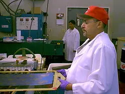
    Photo Chemical Etching Equipment

    As far as our research can determine, most of the companies using this process have at least 20 years in this business, and many of us more than 30 years. Conard was founded in 1965…50 years in the business!

    In addition to the fundamental requirements of quality, value and service, your decision about choosing a photo etching supplier should take into consideration the supplier’s environmental compliance, safety, waste treatment programs and equipment replacement cycles.

    Environmental compliance is generally a state-level activity governing liquid and solid waste products. The federal Environmental Protection Agency (EPA) oversees air quality. Our facility is evaluated regularly by environmental consultants to assure that our compliance procedures are being accurately and consistently followed. This includes specific training in  compliance and safety for new hires and compulsory annual retraining for all production employees.

    We have an onsite waste water treatment facility that enables us to significantly re-use our process water and return it to near-potable condition before discharging it. Our expended etchant is neutralized, relieved of its dissolved metals and re-processed as well.

    In addition to the regulatory and environmental cost burdens, photo etching equipment is not a long-lived asset. Exposure to the acid etching solution, which is both heated and pressurized, takes its toll on the conveyors, bearings, and pumps. Despite continuous preventive maintenance, we routinely replace equipment every four years.

    We continue to invest in the business and its future and have recently completed a plant expansion that adds 25% more space to our production facility.

    When you are considering your options in selecting an etching supplier, ask for a tour of the plant. As Yogi Bera once said, “You can observe a lot just by watching.”

    If you are ready to take the next step:

    Request A Quote
  2. What is the difference between Photo Etching and Chemical Milling

    Leave a Comment

    Photo etching, which is also known as chemical etching, photo chemical etching and photochemical machining (PCM), is a process for fabricating metal components by coating metal in a patterned photo resist and then exposing the metal to an etchant. The metal not protected by the resist will be dissolved and washed away.

    Chemical etching is most often used to produce thin gauge metal parts, sometimes as thin as .0005″. Panel etching can also process ferrous alloys to .040″ thick, copper alloys to .065″, and aluminum to .080″. Photo chemical etching evolved in the 1950s from the printed circuit board industry.

    By using film masters as exposure masks, chemical etching is a meaningful alternative to stamping for many metal applications.

    And it still is today. The exposure masks, or photo tools, can be produced to very high resolutions on laser photo plotters, resulting in even greater precision in the parts produced. Laser direct imaging on glass tools can produce feature sizes less than 100 microns.

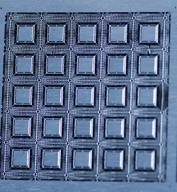
    The range of products manufactured by photo etching continues to grow from extremely fine semiconductor packaging devices to sensor elements up to 24″ x 60″ to giftware and jewelry to industrial components. Chemical etching is exceptionally well suited to manufacturing a wide variety of screens, grid, meshes, and other perforated products.

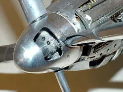
    By comparison, chemical milling is a very different process. Interestingly enough, chemical milling was the process for which Conard Corporation was started. In the 1960s, Pratt and Whitney was forging  propeller hubs in aluminum. Conard’s founder, Richard Huttinger, was a metallurgist at P&W. At that time, the aluminum forging process left a less than optimum surface condition on the parts. There really wasn’t a practical solution for machining these complex surfaces to a finished condition. Huttinger thought it could be done with chemistry. Working from his garage, he eventually developed an etchant that would work consistently and reliably for aluminum.

    Aircraft Propeller Hub

    Chemical milling is often used to reduce the weight of aluminum aerospace components by selectively removing metal from fabricated parts. This is usually accomplished by applying masking material to the non-etch areas on both the inside and outside surfaces. The masked parts are then submerged in a tank of etching solution for a period of time needed to dissolve the desired depth of metal. When applied in this manner, the process may be subject to Nadcap checklist 7108/5.

    A lighter form of chemical milling is sometimes used to prepare metal surfaces for additional finishing operations. These processes may or may not be subject to Nadcap. This application of the process is performed by metal finishing houses and some NDT testing facilities.

    The overall distinction between the processes can be summarized by characterizing photo etching as a fabrication process resulting in the production of components and chemical milling as a modification for altering the surface condition or reducing the weight of fabricated parts.

    For more information about photo chemical machining, these resources may be helpful:

    Comparing Metal
    Fabricating
    Technologies Guide
    FREE Download!

    Download
    FREE Guide on
    Photo Etching Costs

    Or:

    Request a Quote

  3. What is the difference between chemical milling and chemical etching?

    Leave a Comment
    Photo Chemical Etching is a fabricating process for precision metal components.

    As an alternative to “conventional” methods, such as stamping, laser, water jet or wire EDM, chemical etching provides an accurate and economical solution for many precision metal applications.

    The FREE Comprehensive Guide to Photochemical Machining provides detailed information about capabilities, specifications, design rules, cost comparisons and more: Get it here:

    Download the Guide

    How It Works:

    After coating metal in a patterned photo resist and then exposing the metal to an etchant, the metal not protected by the resist will be dissolved and washed away.

    Whether in panel form or reel-to-reel, chemical etching is most often used to produce thin gauge metal parts, sometimes as thin as .0005″. Panel etching can also process ferrous alloys to .040″ thick, copper alloys to .065″, and aluminum to .080″. Photo chemical etching evolved in the 1950s from the then-nascent printed circuit board industry. By using film masters as exposure masks, chemical etching was a meaningful alternative to stamping for many metal applications.

    And it still is today. The exposure masks, or photo tools, can be produced to very high resolutions on laser photo plotters, resulting in even greater precision in the parts produced. Laser direct imaging on glass tools can produce feature sizes less than 100 microns.

    The range of products manufactured by photo etching continues to grow from extremely fine semiconductor packaging devices to sensor elements up to 24″ x 60″ and a wide variety of industrial components.Chemical etching is exceptionally well suited to manufacturing a wide variety of screens, grid, meshes, and other perforated products.

    Chemical milling is a process to selectively alter the characteristics of a fabricated metal part.

    Interestingly enough, chemical milling was the process for which Conard Corporation was started. In the 60s, Pratt and Whitney was forging  propeller hubs in aluminum. Conard’s founder, Richard Huttinger, was a metallurgist at P&W. At that time, the aluminum forging process left a less than optimum surface condition on the parts. There really wasn’t a practical solution for machining these complex surfaces to a finished condition. Huttinger thought it could be done with chemicals. Working from his garage, he eventually developed an etchant that would work consistently and reliably for aluminum.

    Aircraft Propeller Hub

    Chemical milling is often performed on three dimensional parts. Many aerospace components are chemically milled in selective areas to reduce weight without affecting the overall strength and function of the parts. Engine nacelles, cowlings and fairings are typical of the types of parts to be lightened in this fashion.

    Masks for this process are usually computer-cut from pressure sensitive films similar to the vinyl films used for lettering and signage. These patterns are applied by hand to protect metal areas from the acid solution. The masked part is immersed in a tank of etchant for a period of time to affect the material removal.

    The main distinction between chemical machining (etching) and chemical milling is that the machining process fabricates parts and the milling process alters parts.

    Chemical milling may be subject to Nadcap checklist 7108/5.

    Resources for chemical milling services.

    ADDITIONAL RESOURCES

    The Comprehensive Guide to Chemical Machining
    DOWNLOAD

    Introduction to Electroforming
    DOWNLOAD

    Design Considerations for Photo Etching
    DOWNLOAD

  4. Understanding the “Etch Factor” in Photo Chemical Machining

    Leave a Comment

    Etch Factor is Comparable to Tooling Offset

    Like other metal fabricating technologies, photo chemical etching requires adjustments of the nominal dimensions in order for the parts to come out the right size. In other processes, this may be referred to as tooling offset or a similar expression.

    We refer to this adjustment as the “etch factor” and the process of applying the adjustment to the various dimensions of the parts as “compensation.”  If we did not compensate dimensions, the outsides of parts would be too small and the insides of parts would be too big. In some cases, where the metal is thin enough and the dimensional tolerances are generous enough, it may not be strictly necessary to apply the etch factor, however in most cases, we do.

    For more detailed information:

    Download the Guide

    Metal Thickness Affects Etch Factor

    Just as the tolerance band and minimum feature sizes in photo etching are driven by metal thickness, so too is the etch factor. In it’s simplest expression, and assuming a 50/50 etch, the etch factor is thickness/2.

    Let’s take the basic case of a washer. We will call the outside diameter 1″ and the inside diameter .5 inches. If the selected metal is .010″ thick, then we need to adjust the OD to be half the metal thickness larger, or 1.005″. And, similarly, the ID needs to become .005″ smaller or 0.495″ on the phototool. Continuing this example, if the metal thickness is .020″, then the compensated dimensions would be 1.010″ and .490″, respectively.

    Keeping in mind that the clear areas on the phototool represent the actual part, we also apply an “etch band” to the areas to be etched. Depending on the metal thickness and the parts, the etch band that is printed in black on the phototool may be from .020″ to .050″ wide. If a part has large areas of internal cut-outs, we may put an etch band around the cut out and let it fall out, rather than put all of that metal into solution.

    Even though we start with the customer’s nominal data in the CAD file, the output on the phototool itself represents the process factors that are needed to produce the parts correctly as well as avoid putting metal into solution unnecessarily.

    Asymmetrical Etching Ratios

    The 50/50 etch represents the majority of etching applications, and this method is the typical strategy. There are situations where the standard methods must be modified to suit an alternative etching ratio.

    In the cases where an asymmetrical etching ratio ( e.g., 60/40, 70/30, etc) is desirable, each side of the phototool must be compensated separately. In these cases, the etch factor is based on the fractional thickness of the metal, as if it were being etched from one side. So, in the example case of a 70/30 etch on .020″ material, the 70% side (.020″ x .7 = .014″) is treated as the equivalent of etching .028 material 50/50 from two sides. Therefore, the compensation would be .028/2 or .014. The same rationale applies to the minor side, treating .006 from one side as if it were .012 from two sides, or .006″.

    Special Cases in Etching

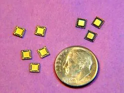
    Although most applications can be served effectively with formulaic solutions for compensation, there are a growing number of designs, especially with regard to semiconductor packaging, that bring additional complexities to the process of compensating for the etch factors. This is particularly true for the so-called “flat, no lead” microleadframes. The “FN” style leadframes, whether “quad” (QFN) or “dual” (DFN), require an heuristic approach to compensation, since the parts involve both partial and full thickness etching in different areas. What may be predicted by calculation, may not prove out in process. This leads to “measure, modify and make again.”

    Photo Etched QFN Leadframe With 72 Leads on a 5 x 5 Die Pad

    As chip technology continues to evolve, newer packaging variants, including thin (T), ultra thin (UT) and extremely thin (X) pose additional challenges to variable compensation.

    Download the Guide
  5. What is the Etch Factor and Why It Matters

    Leave a Comment

    Etch Factor is Comparable to Tooling Offset

    Like other metal fabricating technologies, photo chemical etching requires adjustments of the nominal dimensions in order for the parts to come out the right size. In other processes, this may be referred to as tooling offset or a similar expression.

    We refer to this adjustment as the “etch factor” and the process of applying the adjustment to the various dimensions of the parts as “compensation.”  If we did not compensate dimensions, the outsides of parts would be too small and the insides of parts would be too big. In some cases, where the metal is thin enough and the dimensional tolerances are generous enough, it may not be strictly necessary to apply the etch factor, however in most cases, we do.

    For more detailed information:

    Download the Guide

    Metal Thickness Affects Etch Factor

    Just as the tolerance band and minimum feature sizes in photo etching are driven by metal thickness, so too is the etch factor. In it’s simplest expression, and assuming a 50/50 etch, the etch factor is thickness/2.

    Let’s take the basic case of a washer. We will call the outside diameter 1″ and the inside diameter .5 inches. If the selected metal is .010″ thick, then we need to adjust the OD to be half the metal thickness larger, or 1.005″. And, similarly, the ID needs to become .005″ smaller or 0.495″ on the phototool. Continuing this example, if the metal thickness is .020″, then the compensated dimensions would be 1.010″ and .490″, respectively.

    Keeping in mind that the clear areas on the phototool represent the actual part, we also apply an “etch band” to the areas to be etched. Depending on the metal thickness and the parts, the etch band that is printed in black on the phototool may be from .020″ to .050″ wide. If a part has large areas of internal cut-outs, we may put an etch band around the cut out and let it fall out, rather than put all of that metal into solution.

    Even though we start with the customer’s nominal data in the CAD file, the output on the phototool itself represents the process factors that are needed to produce the parts correctly as well as avoid putting metal into solution unnecessarily.

    Asymmetrical Etching Ratios

    The 50/50 etch represents the majority of etching applications, and this method is the typical strategy. There are situations where the standard methods must be modified to suit an alternative etching ratio.

    In the cases where an asymmetrical etching ratio ( e.g., 60/40, 70/30, etc) is desirable, each side of the phototool must be compensated separately. In these cases, the etch factor is based on the fractional thickness of the metal, as if it were being etched from one side. So, in the example case of a 70/30 etch on .020″ material, the 70% side (.020″ x .7 = .014″) is treated as the equivalent of etching .028 material 50/50 from two sides. Therefore, the compensation would be .028/2 or .014. The same rationale applies to the minor side, treating .006 from one side as if it were .012 from two sides, or .006″.

    Special Cases in Etching

    Although most applications can be served effectively with formulaic solutions for compensation, there are a growing number of designs, especially with regard to semiconductor packaging, that bring additional complexities to the process of compensating for the etch factors. This is particularly true for the so-called “flat, no lead” microleadframes. The “FN” style leadframes, whether “quad” (QFN) or “dual” (DFN), require an heuristic approach to compensation, since the parts involve both partial and full thickness etching in different areas. What may be predicted by calculation, may not prove out in process. This leads to “measure, modify and make again.”

    Photo Etched QFN Leadframe With 72 Leads on a 5 x 5 Die Pad

    As chip technology continues to evolve, newer packaging variants, including thin (T), ultra thin (UT) and extremely thin (X) pose additional challenges to variable compensation.

    Download the Guide
  6. How does Photo Chemical Etching Work and What Can You Do with it?

    Leave a Comment

    Precision Metal Fabricating without Stress

    Photo etching is a “non-conventional” method that fits alongside stamping, punching, laser, and wire EDM for manufacturing many types of metal parts. Suited to many metal alloys, etching eliminates problems common to other processes: burrs and cold working in stamping and punching, heat affected zones or recast layers for laser and wire EDM. It is particularly capable with very thin materials (routinely down to .001″) and both reflective and thermally conductive metals such as aluminum and copper.

    Here’s a quick run down of etching specs and tolerances.

    For more detail:

    Download the Guide

    Chemical machining or etching is a method of fabricating metal components that relies on an acidic solution to dissolve unwanted metal. The photo etching process is used for fabricating metal parts for many different industrial applications including sensors, shields, retainers, flat springs, strain gauges, filters, screens, grids, shims, gaskets and more. For electronics, etching is used to produce a host of metal components used in RF, microwave and wireless applications, as well as lids and leadframes for microelectronics packaging. Photo etched direct bond copper is increasingly used in power electronic applications, particularly in wireless devices. It is also used to produce a host of electrical contacts, buss bars and other electrical interconnect devices.

    Get the picture here : 3-minute video shows the process

    Photochemical machining can be a very economical alternative to stamping, laser or EDM. With inexpensive film-based tooling that can be produced in a day, rapid prototyping is easily achieved. Order minimums are modest and can produce dozens to hundreds of parts at low cost.

    To help engineers and designers in their design-for-manufacture (DFM) decisions, we have published a basic DIY Guide to Estimating Photo Etching Costs. It’s Free!

    How does Photo Chemical Etching Work and What Can You Do with it?

    From Data to Details

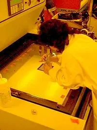
    The basics of the process include creating the photomask, which today is derived from CAD data and output on film from a laser photoplotter. This is known as the phototool. The metal to be etched is carefully cleaned and coated on both sides with a polymer film called photo resist. When applied, the photoresist film is unexposed and this must be done in a yellow safe-light environment.

    Inspection a phototool in the imaging process

    The coated metal and the phototool come together in the imaging process where the black regions on the phototool prevent the exposure of the resist under intense UV light. The unexposed resist is washed away in a developing solution, leaving bare metal in the areas to be etched.

    In the etching process, the exposed photoresist is strong enough to withstand the effects of the ferric chloride etchant. But the unprotected metal is dissolved right up to the edge of the resist. The etchant is sprayed at both sides of the sheet until cut through is achieved. After etching, the resist is washed away in a different solution.

    Photo Etching vs. “the Others”

    Photo etching is also known as chemical etching and photo chemical machining. It evolved in the 1950s as an off-shoot of printed circuit board fabrication, and the production process is very similar.

    Stamping and punching utilize hardened steel tools to shape metal parts. Plasma, laser and water jet cutting utilize directed energy to shape parts. And, wire EDM uses a wire electrode to burn away metal.

    So, just by thinking about the processes, you can easily see the differences. Stamping and punching are sort of “brute force” processes, shearing the metal using powerful presses. Plasma, laser and EDM rely on intense energy, literally burning their way through metal. Waterjet is sort of the “hot knife through butter” option, but you definitely wouldn’t want to get in the way of a pressurized stream of water that can cut through an inch of steel!

    Photo etching, in contrast, would be like running a sheet of metal through your dishwasher and then taking out a sheet of parts.

    Applications for Every Occasion

    So, what can you do you with photochemical machining? You can make very thin metal parts, as thin as .0005″ (yes, five ten-thousandths). You can make fairly thick parts: up to .040″ in ferrous alloys, .065″ in copper alloys, and .080″ in aluminum. You can make parts with funny shapes and lots of holes and it doesn’t cost any extra. You can make some very little parts, as small as .020″ diameter. And, you can make some fairly big parts, up to 24″ x 60″.

    Do you have a project in mind?

    Request A Quote

    ADDITIONAL RESOURCES

    The Comprehensive Guide to Chemical Machining
    DOWNLOAD

    Introduction to Electroforming
    DOWNLOAD

    Design Considerations for Photo Etching
    DOWNLOAD

  7. What are Applications for Decorative Etching?

    Leave a Comment

    When we refer to “decorative etching,” we are distinguishing the application from what we call “precision etching.”  Decorative etching takes many forms, some of which we will cover below, but from the chemical etching process standpoint, we are more focused on appearance than dimensions. Precision etched parts are defined by specific dimensions and tolerances that require particular methods of inspection and sampling.

    When etching decorative products, we include .250″ gauge holes in the phototool. When the gauge pin fits, the etching is done. This method keeps the mechanical inspection process simple and quick. More attention is paid to the aesthetics of the etching, as decorative projects can be quite detailed.

    Chemically etched decorative products are generally shipped from our shop “tabbed in the sheet.” Often times, the sheets are sent for plating, coloring or another metal finishing operation where is is most economical to handle the parts sheetwise.

    The limited inspection requirements and shipping in the sheet have significant benefits in terms of cost. Indirect labor (inspection, packaging) is virtually nil. Decorative products are our most economical sheets. We typically ship decorative within two weeks since there is little to no engineering involvement.

    The most commonly used alloy for decorative etching is brass which we stock in both polished and mill finish. Stainless steel, aluminum and copper are sometimes used as well. Most decorative applications are in .015/.016 or .020″ thick metal. Although, we have etched projects on .005″ and up to about .060″. We are installing a new etching line specifically for silver. The equipment is on order and will be installed in May 2013.

    The three major categories of chemically etched decorative products are giftware, jewelry and scale models.

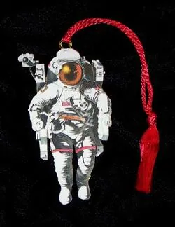
    Giftware takes many forms, including bookmarks, ornaments, picture frames, inlays, letter openers, charger plates and so forth. Giftware finishes may include electroplating, enamel, cloisonee or digital color. Some trophy and award elements are produced by photo etching as well. Giftware often encompasses specific commemorative themes including historic places, people and events. For our annual bookmark series, we highlight themes related to manufacturing and technology.

    Jewelry items made by etching include earrings, pendants, charms, bracelets, and pins. There is an endless variety of distinctive themes and designs created for jewelry, some of it very complex and delicate. Chemical etching may be the only practical means of fabricating them. In some designs, the etched element is “dapped,” which is a simple spherical embossing to give the parts a “third” dimension. Finishing options are similar to giftware and may include precious metal plating.

    Photo Etched and Digitally Colored Brass Bookmark

    Scale model kits are among the most intricate of the decorative etching projects. Some kits may contain hundreds of small parts tabbed to frets. Most of the model kits are in brass, often .005″ to .008″ thick. The parts are designed with half etch lines so the elements can be folded into 3-D structures. Popular subjects for metal scale models include railroads, ships, planes, military vehicles, buildings, bridges and more. We have etched metal accessories for action and anime figures as well as cult movie paraphernalia.

    Additional uses for decorative etching include architectural elements and lighting diffusers; affinity tokens and emblems, durable signage, wall art, clock faces and hands, belt buckles and ornamentation for clothing, eyeware and home furnishings.

  8. Why use Photo Etching for Microelectronics?

    Leave a Comment

    Mini, micro, nano. Things are getting smaller all the time.

    Here are some things you can relate to:

    • A credit card is about .020″ thick (twenty thousandths of an inch or ” 20 mils”)
    • A human hair or a sheet of paper is about .005″ thick (five thousandths or 5 mils)
    • Aluminum foil in your kitchen is about .001″ thick (one thousandth or 1 mil)
    Photo etched microelectronics packaging

    These dimensions are not small enough to describe what’s happening in the world of electronics. For that, we need to go metric, and then some. A meter is 40 inches. A millimeter is .040″ (forty thousandths). A micron (or micrometer) is 40 millionths of an inch. And a nanometer is 40 billionths of an inch.

    When I was in high school, the smallest semiconductor transistor (the basic building block of electronics) was 10,000 nanometers. Today, the transistors on the chips in our cell phones are about 20 nanometers. Within a couple of years, they expect that size to drop to about 10 nanometers. And last year, some researchers in Australia created a transistor that is only 0.1 nanometers.

    The CPU chips in most of our computers and tablets are about 1 inch square and contain over a billion transistors etched in silicon. Which is all well and good, but how do you connect these tiny things to the outside world?

    Metal stamping can’t achieve the feature resolution needed. Thus, photo etching is playing a much bigger role in microelectronics packaging. And, the needs being driven by the shrinking size of semiconductor features is pushing etching technology further.

    I contacted Richard Sayer of International Phototool Company LLC and asked him about the state of the art in phototooling. His comments are very informative:

    “With polyester film, the smallest image sizes that we could achieve on a production basis was about 8 microns on linear features, and 5 to 6 microns on a best-efforts engineering-mode basis. With respect to round/square/hexagonal features, this technology allowed for about 10 micron diameter pads. These dimensions were achievable only the Barco Silverwriter laser photoplotter with souped-up “Eagle Optics”, plotting at 65,000 dpi resolution. Otherwise, the best available capabilities in commercial production at 40,000 dpi resolution yields feature sizes in the 10 micron (0.0004”) range on linear patterns and 15 microns (0.0006”) on round/square/hexagonal pads. We only offer imaging up to 40K dpi resolution at this time.

    With respect to chrome or iron oxide on glass, we are nowadays able to produce direct-write laser photomasks with linear and round feature sizes down to 3 microns and smaller, with 6-sigma tolerances at +/- 10% of the CD (critical dimension) size. Actually, we’ve been able to supply these for quite some time, but new technology brought to market within the past few months has allowed us the luxury of rapid throughput (hours vs. days) and much lower prices. Of course, we still produce photomasks with much larger feature sizes, but the low cost and rapid throughput of photomasks with smaller images has allowed for somewhat of an explosion of activity in the areas of MEMS and Microfluidics research and production. Standard mask sizes from 2.5” to 7” square, as well as large area photomasks from 300, 350, 400, & 450 mm square, with custom sizes up to 24” x 28” are now more readily available and with lower prices than ever before.

    Download The Design Guide
  9. What are the Advantages of Photo Etched Screens?

    Leave a Comment
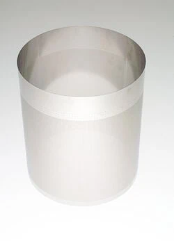
    Photo Etched, Formed and Welded Stainless Filter

    Photo etching is an ideal solution for creating parts with lots of holes. In photo etching, the complexity of the part has no effect on tooling cost, processing or part cost. Whether the part is a solid shape or a screen, the etching process is exactly the same. As I often say to people, “we only charge you for the first hole, the rest of them are free.”

    Unlike any other metal cutting process, chemical etching produces holes that are completely burr-free and the metal has not been subjected to mechanical or thermal stress. Photo etching can easily produce grids and screens that have variable patterns, with or without solid borders, and in virtually any shape at no additional cost.

    Photo etched screens, filters and grids find applications in so many different industries. From laser printers, to smoke detectors, to batteries, to scientific, medical and industrial instruments, and many more, photo etching is the process of choice for producing burr- and stress-free metal parts.

    The photo etching process produces consistent quality, screen after screen, because there is no mechanical tool wear and the metal itself is never subjected to extreme heat or shearing forces. Screens can be chemically etched in metals as thin as .001″.

    Photo etched screens can be flat or formed. Many customers take the parts in the flat state and form them at assembly. Some etched screens and grids are overmolded with plastic for various applications. Depending on the configuration, etched filters are used for screening solids, liquids and gases.

    Etched screens, filters and grids are produced in a wide variety of alloys including stainless and carbon steel, copper, brass, bronze, aluminum, nickel, and molybdenum.

    We have a lot of people ask us about screens, so we put together a list of the most popular “FAQs” about photo etching screens, filters and grids.

    Photo Etched Stainless Toner Grid

    Q: What are the limitations for etched screens?
    A: The minimum hole size needs to be, preferably, 120% of the metal thickness and the minimum ligature between holes is not less than the metal thickness and never less than .005 inches.

    Q: What is the largest screen you can make?
    A: Our equipment can process screens up to 24” x 60”

    Q: What are the thinnest and thickest materials you can process?
    A: .001 inches in most alloys and up to .080 inches in aluminum.

    Q: How much do etched screens cost?
    A: For common alloys (stainless, copper, brass, aluminum) between .010 and .020 thick, you can expect costs between .20 and .30 per square inch, assuming 120% minimum hole size.

    Q: How much does tooling cost?
    A: For screens up to 24” x 24”, generally, $265.00

    Q: Do you have any standard screens?
    A: No. Everything is made to customer specifications.

    Q: Do the holes have to be round?
    A: No. The holes can be virtually any shape and they don’t have to be the same shape. Any collection of shapes can be made. The caveat is that the minimum radius is equal to the material thickness and the 120% rule applies to the narrowest area of an opening.

    Q: Can screens have solid borders and does it cost extra?

    A: Screens can be any shape, any number of holes, with solid borders or not, and the only cost factors are the length, width, thickness and alloy. One hole, a million holes…makes no difference in the co

  10. What are the Problems of Cutting and Photo Etching Aluminum?

    Leave a Comment
    Photo Etched Aluminum Heat Sink

    One of the lightest metals, aluminum, is one of the more challenging alloys to to process. This post will compare laser and plasma cutting with photo etching with regard to cutting aluminum.

    The biggest problem with laser and plasma cutting is heat. Aluminum melts at about 1200 degrees F. The plasma stream is about 25,000 degrees. By definition, laser cutting is a process of melting the material in its path, so the work piece will be subjected to high temperatures. The thermal impact of these processes can produce a recast or slag layer, known as the Heat Affected Zone (HAZ). This thermal exposure can alter the properties of the metal, which is generally undesirable. By comparison, the photo etching process rarely gets warmer than 150 degrees, about the same as your dishwasher.

    Dimensional accuracy is another area where there are meaningful differences between laser, plasma, and photo etching.

    On plasma cutters, the beam width is determined by the nozzle size, with a ratio of 1.5 to 2X nozzle diameter to beam width. It is possible to put a .001 nozzle on a plasma cutter to produce a .002 beam, but you can’t push very much power through that aperture. Dimensional accuracy of plasma cutters runs about +/-.015-.020″.

    On laser cutters, the beam width is determined primarily by the optics. For metal cutting machines, typical beam widths of .006-.016″. (Laser marking machines can have much smaller beams.) Laser cutters can achieve +/-.005″ dimensional accuracy. Two additional issues with laser cutting aluminum are optical reflectivity (aluminum is shiny) and thermal conductivity (the metal dissipates the heat the laser is trying to generate.)

    In photo etching, dimensional tolerances are +/-15% of material thickness. For metals that are .032″ or less in thickness, photo etching will easily produce tolerances that are tighter than +/-.005″.

    The etching challenge with aluminum is that is it a very active and reactive metal. It oxidizes readily and actually becomes fuel for the etching reaction. Another problem is that aluminum will etch in both acids and bases. The solution used to dissolve the acid-resistant photo resist is a base. In the process design for etching aluminum, allowance has to be made for the slight but inevitable etching during the stripping process.

    Photo etching has proven to be a versatile and cost effective method of fabricating thin-gauge metal parts in many alloys. The vast majority of metals can be successfully photo etched using ferric-chloride etchants, which are among the easiest, safest and most economical to use. However, ferric chloride does not produce the best results on aluminum.

    Etching aluminum is the foundation of Conard’s business. In the early 1960’s, Dick Huttinger, a metallurgist for Pratt and Whitney, was trying to find a better way to finish the surfaces of forged aluminum propeller hubs. At that time, CNC machining was neither sufficiently sophisticated nor cost effective for the task. Huttinger believed that it could be done chemically and developed the methodology that we continue to use to this day.

    Our General Manager, Art Long, has worked in this industry for more than 30 years and is well familiar with the challenges of etching aluminum. “The biggest problem is edge consistency, sometimes the edge would look smooth and other times it would appear very rough. It was difficult to control the quality of the etchant from one bath to the next and from one alloy to the next,” said Long. “When I joined Conard in 2003, I noticed that the aluminum etching capabilities were head and shoulders above the previous companies I had worked for. The product had consistently smooth sidewalls and was precise in a wide range of different aluminum alloys and thickness.”

    For more information, contact us at 860-659-0591 or:

    Request A Quote