Exit

Author Archives: Conard Corporation.

  1. Why Sensors Benefit From Precision Metal Etching

    Comments Off on Why Sensors Benefit From Precision Metal Etching
    Why Sensors Benefit From Precision Metal Etching
    Photo etching is a powerful option for OEMs looking for a supplier of precision component parts for sensors.

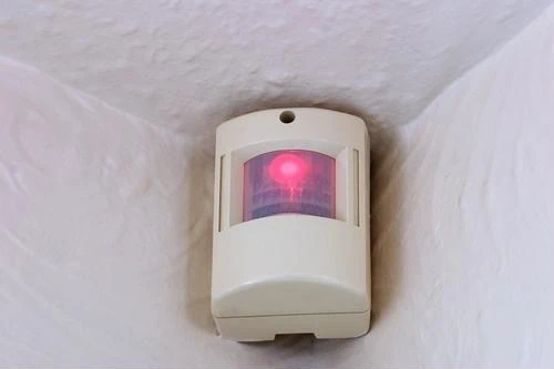
    Devices, equipment and consumer products are increasingly equipped with sensors and other communicative technologies. These sensors – and their components – interact mechanically with their environment and electronically with the system or device to which they “report”. Here are a few common applications for sensing/measuring technology today:

    • Scientific instrumentation – atmospheric sampling, strain gauges, mass spectrography, chromatography, photometry and other lab equipment.
    • Industrial machinery – flow and capacity sensors, pressure membranes and electronic traceability.
    • Consumer goods – kitchen appliances, smart thermostats, automobiles, smoke and carbon monoxide detectors, etc.

    Because sensors must be small enough to be noninvasive to the normal functioning of the device, yet still powerful enough to perform at an optimal level, fabrication processes must be able to accommodate very strict design standards. Photo etching is one process that can tackle these difficult manufacturing challenges. Here are some of the key reasons why:

    Modern Medical and Scientific Equipment Rely Heavily on Sensors
    Modern medical and scientific equipment rely heavily on sensors.

    Cost-effective at any production volume
    Machining complex flat metal parts can get very expensive if you’re using conventional processes such as laser cutting, stamping or wire EDM for large production runs. This is mostly because the tooling costs – creating dies for stamping, for example – with these processes increase along with volume. Photo etching doesn’t run into that issue because we don’t have any “hard” tooling.

    Using a CAD file with your part’s design, we generate a phototool. This is a stencil in the shape of your finished part printed on dimensionally stable mylar using an 8,000-dpi photoplotter. Since UV light is the phototool’s only working exposure, there is no tool wear in the traditional sense of a die or drill getting worn out from multiple uses. The phototool can be created for about $300 or less and be ready within a few hours. Because we’re just printing them, phototools can be easily regenerated for multiple production runs without running your costs up.

    Part complexity is a non-issue
    During the etching process, the phototool is laminated to both sides of a sheet of metal, leaving the metal bare where the part is to be etched. The sheet is exposed to the etching solution (usually ferric chloride), and the exposed metal is dissolved all at once, leaving the final part.

    Because the “machining” happens simultaneously, we can create very intricate parts – with odd shapes or lots of holes – quickly, easily and accurately. Conventional processes like CNC punching, laser and EDM can only work on one small localized area of the part at a time. The more complex the part, the more time it takes – another major cost driver.

    Dimensional accuracy
    For sensors and other microelectronics to work properly, each component and subassembly needs to be precisely made. They have to fit into small spaces, and a part that’s even slightly out of tolerance can throw the whole thing off. Photo etching is able to hold tight tolerances, so your parts come out to your specifications without worrying about adverse effects created by conventional processes like thermal and mechanical distortions or burrs. The tolerances we hold depend on the thickness of the metal sheet:

    • Minimum dimensional tolerances of +/-.001″ are achievable on metals up to .005″ thick.
    • For metal over .005″ thick, minimum dimensional tolerances will be +/- 15% of metal thickness.
    • Location tolerances will be within +/-.001″ of drawing nominal.

    To learn more about photo etching, call us at 800-443-5218 or email us at sales@conardcorp.com and we can get started working on your designs!
    Request A Quote
  2. Why Photo Etching Matters in the 21st Century

    Comments Off on Why Photo Etching Matters in the 21st Century
    E001

    The accelerating evolution of 3D printing technologies is garnering a lot of headlines. And, while it is likely that these technologies will enable the manufacture of an astounding variety of products, it is also likely that 3D printing will continue to be slow and costly compared to other metal fabricating processes.

    Advances in electronics technologies are also accelerating. Just this week, a group of researchers at UC Riverside announced the development of a process to produce anodes for lithium ion batteries from sand. This discovery could increase the charge capacity of these batteries by a factor of three. As electronic devices become smaller, more powerful and more interconnected, the need for increasingly delicate yet robust means of connecting semiconductor chips to their inputs and outputs only grows.

    Photo etching accommodates fabricating a wide selection of metal alloys, including many copper- and nickel-based alloys that are widely used in microelectronics packaging devices including leadframes, lids and contacts. The ability to photo etch leadframes and other contact devices in arrays facilitates automated wire bonding of the semiconductor dies.

    Smaller, more powerful and power-hungry devices benefit from the dimensional stability and heat dissipation characteristics of direct bond copper on ceramic, usually aluminum oxide, or aluminum nitride for even higher heat dissipation. Photo etching is the only practical solution for creating circuit patterns on DBC substrates. DBCs are usually etched and then laser scribed ( and sometimes drilled) for singulation. Common plating options include electroless nickel, either alone, or with immersion gold. We can provide end-to-end support for these services.

    Chemical etching finds a broad swath of uses across the entire spectrum of wireless technologies, with new devices and designs emerging, it seems, daily.

    We receive frequent inquiries about etching applications in alternative power; new display technologies; medical, scientific and industrial instruments and sensors; as well as astoundingly long-lived aerospace and defense systems.

    Between the newest of the new and the durable legacies, photo etching is a relevant and versatile process for producing precision metal components. After nearly 50 years in this industry, we know we haven’t seem it all.

    Digitally driven technologies like lasers, waterjets and now 3D printers, are less about replacing other processes and more about expanding the ranges of things that can be done more easily and effectively.

    If you have an application you would like us to look at: Request a Quote

    If you would like to learn more about the photo etching process: Download Now
    Engineering Design
    Guidelines

    And, if you just want to talk, call me at 800-443-5218.

  3. Why OEMs Rely on Photo Etching for Key Applications

    Comments Off on Why OEMs Rely on Photo Etching for Key Applications

    From semiconductors to fuel cells to filtration to medical devices –and many more– major OEMs, names you will instantly recognize, use photo etched precision metal parts in key applications. Given the vast array of metal fabricating resources and technologies available to leading OEMs, why would they choose photochemical etching for critical elements of their products?

    The primary drivers for the photo etching option include:

    • It’s the best way to produce a given part. Other processes may leave undesirable vestiges or affects on the metal.
    • It’s the only way to produce a given part. Other processes may be incapable of resolving certain levels of detail, or may be ill-suited to processing very thin materials or certain alloys.
    • It’s the most economical way to produce a given part. For fine filtration products and many semiconductor packaging devices, among others, photo etching is far more cost effective and produces a superior product compared to other possible solutions.
    • It’s the best balanced option. Low cost tooling in a day (compared to stamping) and low effective unit costs compared to laser, water jet or wire EDM.

    Unfortunately, photo etching is also the least known option in metal fabricating. Educating designers and engineers about the capabilities of photochemical machining (yes, this is the “formal” name) is our biggest job.

    Applications where photo etched components are widely used include:

    • Fuel cell stacks and flow plates
    • Rechargeable batteries
    • Heat transfer/exchange devices
    • Turbines and bearings
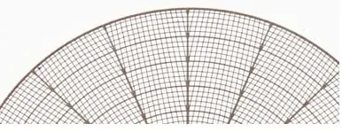
    • Filters, screens, grids and meshes
    • Analytical instruments for scientific, medical and industrial uses
    • RF, microwave and wireless communications
    • Mechanical linkages and electrical interconnects
    • Microelectronics and power electronics
    • Controls, actuators, sensors
    • Waveguides, seals, gaskets, shims
    • Flexible heating elements and magnetic field coils

    Industries utilizing etched metal components include:

    • Aerospace & Defense
    • Automotive
    • Consumer Electronics and Appliances
    • Energy
    • Food Processing
    • Chemical Processing
    • Water and Waste Processing
    • Medical
    • Communications
    • Semiconductors and Electronics
    • Industrial and Scientific Instruments and Controls
    • and many more
    Nickel Grid

    The potential applications for PCM are only limited by the relatively small community of people who are familiar with the process. Our goal is to spread the word and share the wealth.

    Here’s an introduction to Understanding Etching Costs and some information about tolerances

    For more technical info: Download Now
    Engineering Design
    Guidelines

    To reach me: 800-443-5218 or kstillman@conardcorp.com.

  4. Why Engineers and Designers in the Know Love Photo Etching

    Comments Off on Why Engineers and Designers in the Know Love Photo Etching

    A “Multi-Tool” for Metal Fabricating

    Modern solid modeling systems give engineers and designers of precision metal components a wide variety of options for fabricating their creations, whether it be stamping, punching, or digital cutting via laser, plasma or waterjet. However, none of these software platforms has any information at all about photo chemical machining.

    We’ve met a good number of engineers over the years who needed to fabricate parts that weren’t suitable or practical for any of the methods they –and their software–knew about. We have witnessed many looks of wonder, and even awe, when they realized that photo etching was not just the solution they needed, but was the best solution for their projects.

    Why Do they Keep Coming Back?

    Could it be love?

    One of our longest customer relationships goes back to the 1970s. We have produced tens of thousands of pieces for more than 400 different parts for them in the past 40-plus years.

    In any given year, 80% of our business is from long-term customers. Last year, we shipped more than 2.3 million pieces of more than 600 unique parts to 170 customers.

    Customers had us create nearly 200 new part designs last year.

    How You Can Be in the Know, Too

    All of the “good stuff” is right here in the Comprehensive Design Guide. 

    It boils down to a few simple rules and ratios that are mostly common sense and a little bit of fluid dynamics. No months spent learning some massive and complicated system. You can begin your photo etching design career in minutes.

    Check Out the Data

    I wondered if I was engaging in confirmation bias in my assertion that when engineers and designers learn about the capabilities of photo etching, they look for every opportunity to make another photo-etched part.

    I did a quick take among our most active precision customers and this is what I found:

    • A customer in the RF/electronics industry has designed 172 etched parts
    • A customer in the aerospace/electronics industry has 158 parts
    • A customer in the RF/microwave sector uses 84 etched parts
    • A job shop (laser and die cutting) has chosen the etched option 37 times
    • A customer in thermal management tech uses 19 etched parts
    • A customer in industrial springs has converted 31 parts to etching
    • Microelectronics and  semiconductor packaging components encompass more than 300 distinct parts
    • We have produced more than 400 different braze foil pre-form designs for a number of customers serving aerospace applications.
    • And, there are more than 500 etched designs used in power generation and storage applications.

    We also have dozens of customers that have been buying the same handful of etched parts for years, and in some cases- decades.

    And, while there may be some confirmation bias in my assertion, there is also evidence to support the contention that engineers who know about etching* use it as frequently as they can.

    Want to Be on the Inside?

    We can help.

    Here’s a link to our most popular white papers.

    Or you can watch a 3 minute Youtube video here.

    You can email your questions to me  or Max.

    And, we’re still happy to talk on the phone:  800-443-5218.

  5. Why Engineers and Designers Love Photo Etching

    Comments Off on Why Engineers and Designers Love Photo Etching

    When Your Only Tool is a Hammer…

    As the old saying goes, every problem looks like a nail. Modern solid modeling systems give engineers and designers of precision metal components a wide variety of options for fabricating their creations, whether it be stamping, punching, or digital cutting via laser, plasma or waterjet. However, none of these software platforms has any information at all about photo chemical machining.

    We’ve met a good number of engineers over the years who needed to fabricate parts that weren’t suitable or practical for any of the methods they –and their software–knew about. We have witnessed many looks of wonder, and even awe, when they realized that photo etching was not just the solution they needed, but was the best solution for their projects.

    When They Keep Coming Back…

    Could it be love?

    One of our longest customer relationships goes back to the 1970s. We have produced tens of thousands of pieces for more than 400 different parts for them in the past 40-plus years.

    In any given year, 80% of our business is from long-term customers. Last year, we shipped more than 2.3 million pieces of more than 600 unique parts to 170 customers.

    Customers had us create nearly 200 new part designs last year.

    What Do You Need to Know…

    All of the “good stuff” is right here in the Comprehensive Design Guide. 

    It boils down to a few simple rules and ratios that are mostly common sense and a little bit of fluid dynamics. No months spent learning some massive and complicated system. You can begin your photo etching design career in minutes.

    Is It Really True?

    I wondered if I was engaging in confirmation bias in my assertion that when engineers and designers learn about the capabilities of photo etching, they look for every opportunity to make another photo-etched part.

    I did a quick take among our most active precision customers and this is what I found:

    • A customer in the RF/electronics industry has designed 172 etched parts
    • A customer in the aerospace/electronics industry has 158 parts
    • A customer in the RF/microwave sector uses 84 etched parts
    • A job shop (laser and die cutting) has chosen the etched option 37 times
    • A customer in thermal management tech uses 19 etched parts
    • A customer in industrial springs has converted 31 parts to etching
    • Microelectronics and  semiconductor packaging components encompass more than 300 distinct parts
    • We have produced more than 400 different braze foil pre-form designs for a number of customers serving aerospace applications.
    • And, there are more than 500 etched designs used in power generation and storage applications.

    We also have dozens of customers that have been buying the same handful of etched parts for years, and in some cases- decades.

    And, while there may be some confirmation bias in my assertion, there is also evidence to support the contention that engineers who know about etching* use it as frequently as they can.

    *You Can Be One (who knows about etching), too!

    We can help.

    Here’s a link to our most popular white papers.

    Or you can watch a 3 minute Youtube video here.

    You can email your questions to me  or Max.

    And, we’re still happy to talk on the phone:  800-443-5218.

    Request A Quote  today!  

  6. Why Designers Should Consider Photo Etching

    Comments Off on Why Designers Should Consider Photo Etching

    Designers of precision metal components may face constraints when considering the more well known options for fabricating many flat metal parts. Metal stamping, by far the largest segment of this market, requires hard metal tooling that can produce burrs and cold working. Laser cutting and wire EDM can impart excessive heat to the work object that may alter the characteristics of the metal. And in all of the cases, the more complex the part is the greater the impact on cost.

    Why Designers Should Consider Photo Etching

    Photo etching avoids all of those challenges. Phototools run about $300, no matter how complex the part, and can be had in a day or two.

    In the chemical etching process, there is no metal-on-metal contact that is pretty much the definition of metal stamping. Therefore, burrs and cold working simply can’t happen.

    And, the highest moment of heat in the etching process is about 165 F, for a few seconds and about 135 F sustained. So, compared to lasers and EDM at thousands of degrees sustained through the processes, photo etching is barely even warm.

    Photo etching is suitable for a wide variety of alloys, including some that are less compatible with other processes. For example, molybdenum-a refractory metal- is difficult to stamp because it can fracture. Aluminum is challenging for lasers because it is reflective, and copper’s high thermal conductivity also reduces laser’s efficiency. Chemical etching is also more capable in processing very thin materials, routinely down to .001″ thickness. Etching is also effective in fabricating braze foil pre-forms in alloys of aluminum, copper, nickel, indium and silver.

    In a study conducted under the auspices of the Photo Chemical Machining Institute, a trade organization, cost analyses were performed across multiple fabrication methods, including stamping, laser, water jet, wire EDM and photo etching, using multiple parts of similar size and increasing complexity. We’re happy to share that with you here.

    The major key to photo etching cost efficiency is dimensional tolerances, which are driven by metal thickness. The standard tolerance band is +/-15% of metal thickness, so that covers drawing block tolerances of +/-.005″ for metal thickness up to .032″. The practical minimum tolerance is +/-.0015 on metals up to .010″.

    This chart illustrates the relationship between tolerances, sheet sizes and costs for photo etching. The clear conclusion is that when your design can accommodate a wider tolerance band, there are significant advantages in costs. The point of leverage is the larger the sheet size, the more parts per sheet, since the unit of labor is the sheet.

    If you would like a no-obligation drawing review, you can send it to me directly at kstillman@conardcorp.com. Or upload your file here and we’ll get back to you right away.

  7. When You Need a Whole Lot of Holes…

    Comments Off on When You Need a Whole Lot of Holes…

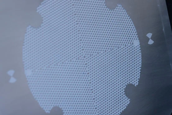
    Many engineers and designers have embraced photo etching, also known as chemical etching or photochemical machining, as their go-to option for making metal filtration, grids and screens.

    Some of the benefits of etching include:

    Precision and Accuracy:

    Photo etching allows for high precision and accuracy in creating patterns and designs on metal surfaces. This is crucial for manufacturing filtration products with specific and complex geometries.

    Fine Detail:

    Designers can create fine details and intricate patterns on metal sheets that would be prohibitively difficult to produce with stamping or punching, and exceptionally expensive in cycle time for laser or plasma.

    Customization:

    Manufacturers can easily create perforated products with varying mesh sizes, shapes, and configurations to meet specific filtration/screening requirements.

    Burr-Free and Stress-Free:

    Mechanical cutting methods often require secondary processing to remove burrs. Photo etching produces burr-free and stress-free metal components. Engineers value this property as any burrs or residual stresses could affect the performance and integrity of the filters.

    Material Versatility:

    Photo etching is compatible with a wide range of metals, including stainless steel, aluminum, and nickel and copper alloys. Nickel and copper have become increasingly popular alloys for battery anodes and cathode

    Cost-Effective for Prototyping:

    For a few hundred dollars, designers can prototype multiple configurations at one time to accelerate the product development process.

    Tight Tolerances:

    Photo etching tolerances are typically +/- 15% of metal thickness to a practical minimum of +/-0015” for metal foils .010” thick and less.
    Reduced Material Waste: The process is highly efficient and produces minimal material waste compared to traditional machining methods. This contributes to cost savings and aligns with sustainable manufacturing practices.

    In summary, photo etching offers a combination of precision, customization, material versatility, and cost-effectiveness, making it well-suited for the manufacturing of metal filtration products where intricate designs and high precision are essential.

    For more information, check out some of our popular resources here.

    Download the Guide
  8. What You Need to Know about Self-Managing Decorative Etching Projects

    Comments Off on What You Need to Know about Self-Managing Decorative Etching Projects

    As a commercial etching facility, our primary purpose is to get the work out the door on time and in conformance with customer specifications. Over 90% of the work we do is defined as “precision” work: we work to engineering drawings and specifications, and there are inspection, conformance and documentation requirements. Meeting these kinds of requirements is why we have engineering staff and an entire inspection department.

    What You Need to Know about Self-Managing Decorative Etching Projects

    As it happens, the very same metal etching process that produces precision parts for industrial applications is also well suited to create products for designers of jewelry, giftware, scale models and other aesthetic purposes. The big difference is that the quality requirement is much simpler:  the parts need to look good.

    • We have a standardized approach to processing decorative etching work at fixed prices.
    • We use one sheet size:  18″ x 24″.
    • We offer four thicknesses of metal:  .016″, .020″, .025″ and .032″. As a point of reference, .020″ is the thickness of a credit card. .005″ is the thickness of a sheet of paper.
    • Standard decorative is available in four metals:  stainless steel, brass, copper and aluminum.
    • Customers who prefer other alloys, such as sterling silver, nickel silver, carbon steel, or bronze must supply it themselves.

    Since all we are doing is the etching, the customer takes responsibility for design work and also purchasing and having the phototool produced. We are happy to refer customers to resources for both of these processes.

    Standard decorative is priced to ship tabbed in the sheet. We routinely ship to other service providers, such as electroplating, screen printing and finishing (cut out and deburr), however the responsibility for arranging orders with these providers rests with the customer.

    Here are the key things to know:

    • The customer is responsible for design
    • The customer provides the phototool
    • The customer arranges for additional services, if desired
    • All we do is the etching

    Here are some additional resources:

    Download the 2014
    Simple Parts Per Sheet
    Count for
    Decorative Products

  9. What to Know about Photo Etched Sidewalls

    Comments Off on What to Know about Photo Etched Sidewalls

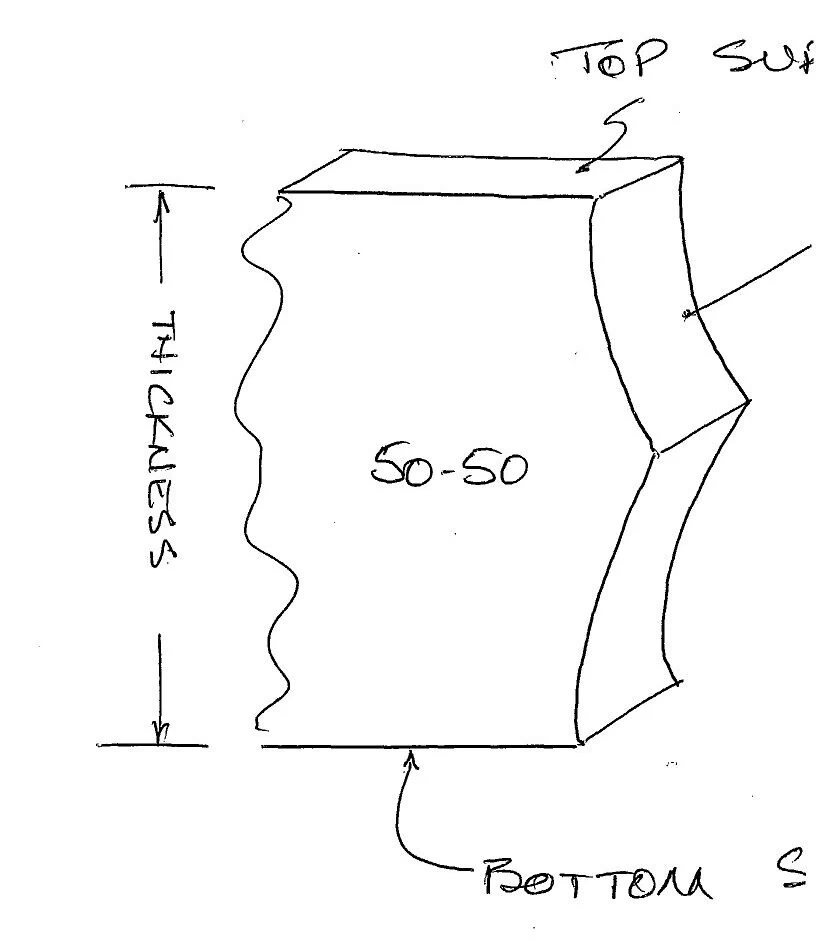
    Different metal cutting processes produce different effects at the cut line. Stamping and punching can leave a deformation and a burr on the die side of the plate. Laser, plasma and EDM can leave a heat-affected zone or recast layer. Abrasive slurry water jet can leave a somewhat erose sidewall. And photo chemical machining has its own sidewall artifact that we call a “feather.”

    Most often, photo etching is done from both sides equally and at the same time as a “50/50″ etching ratio. As the etchant penetrates from each side of the metal, the cutting path widens at the surface as it deepens. This effect occurs at the predictable rate of .00025″ in width per .001″ of cut depth. The feather reaches its maximum at the point of breakthrough. To calculate the feather, multiply .00025” by half the metal thickness.

    Sidewall

    Unless otherwise specified, we measure to the feather. If your application is more sensitive to total surface area, we need to know that so we can discuss with you the implications with regard to mechanical dimensions at the feather.

    There are times in photo etching that we use other etch ratios, such as 60/40 or 80/20. Usually, the applications for this involve filtration to produce a hole on one side that is smaller than the metal thickness would typically allow. The rule of thumb is that the minimum hole size is 115% of the metal thickness.

    With a ratio etch, we treat each side of the metal as if it were a different thickness. If we wanted to use an 80/20 ratio on .010 material, we would treat the 20% side as if it were .004″ thick and the 80% side as if it were .016 thick. With this ratio, we could put a .005″ hole on the 20% side and the 80% side would be about .018. The center distances on the holes would have to be the 80% side plus the overall metal thickness.

    Using a ratio etch, the feather will move to the new breakthrough line, in our example it would be .002″ from the 20% side of the sheet and the feather will be driven by the 80% side and will therefore be .00025″ x 8, or .002″.

    For more information about desgining for photo etching, please feel free to download information from our website:

    Download Now
    Engineering Design
    Guidelines

  10. What’s Hot in Photo Etching

    Comments Off on What’s Hot in Photo Etching

    When the heat is on, many look to photo etching to move it around or make something useful of it–like electricity.

    One of the oldest thermal applications for etching is heat sinks, devices that help remove heat from vulnerable electronic components. Heat sinks are generally passive devices, relying on air conduction to radiate heat away. Etching offers the ability to create pin- or vane-like structures that increase the effective radiating surface area without increasing the actual footprint of a device.

    • Etched aluminum circuit board heat sink
    H009-1
    • Etched aluminum “pin fin” radiator plate
    What's Hot in Photo Etching

    “Cold plates” get an assist from a transfer medium such as anti-freeze to absorb excess heat and shuttle it away to be chilled and recycled. In a conventional radiator, the coolant is carried in tubing, often surrounded by metal vanes to help dissipate heat. In a cold plate the tubing is replaced by etched channels in copper or aluminum plates that are bonded together channel-to-channel to create tubes, of a sort, through which coolant is pumped.

    Power generation and storage are also beneficiaries of the capabilities of photo etching. Fuel cells, batteries and evolving distributed generation technologies require part geometries that are uniquely realized by chemical etching.

    Proton exchange membrane (PEM) fuel cells take advantage of photo etching’s agnosticism with regard to part complexity vs. cost to produce very intricate membrane elements for both generating electricity and electrolyzing water to produce hydrogen.

    Nickel-metal hydride and lithium ion power cells are the batteries of choice for space-based applications. Both rely on photo etching for critical components.

    • Etched nickel cell grid for NiMH batteries
    A001

    Thermal cycles are also useful in power generation. The “waste heat” of combustion is captured and converted to “work” (in the parlance of thermodynamics) as an additional stage of generation, often through steam turbines.

    However, a number of evolving strategies are taking advantage of the ability of photo etching to create complex partial-depth etched structures and patterns that are central features of new distributed power generation technologies that take advantage of thermal cycles without the rotating machinery.

    There are growing applications in power electronic components that are built on direct bond copper circuit materials. These are constructions of aluminum oxide (alumina) or aluminum nitride ceramic that have copper foil diffusion bonded on both sides. The ceramic dissipates the heat generated by the device, enabling both higher power applications and longer service life.

    Etched direct bond copper on ceramic power electronics base

    Direct Bond Copper

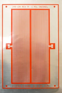
    A long-time application for etching is in flexible resistive heating elements. Typically an electrically conductive material such as Inconel, stainless steel, nickel or copper is bonded to a non-conductive substrate such as silicon rubber, fiberglass or a polymeric material such as polyimide or polyester. The element pattern is etched into the metal down to the substrate, and the resulting circuit is usually affixed with electrical leads and encapsulated with another layer of non-conductive material. These types of devices find many applications in aircraft, both as de-icing boots for leading edges of the airframe or propellers, as well as preventing freezing in other systems on board.

    Etched Inconel on silicon rubber flexible heater element

    Foil Heaters

    So, if you have a “hot” situation, you can keep your cool with photo etching. Contact us for more information.

    For more detailed information on photo chemical machining, download our free comprehensive guide:

    Download the Guide