Exit

Author Archives: Conard Corporation.

  1. Why is Photo Etched Direct Bond Copper (DBC) Becoming so Popular?

    Leave a Comment
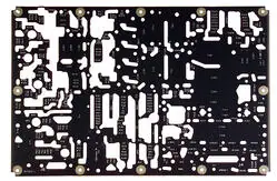
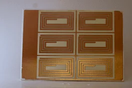
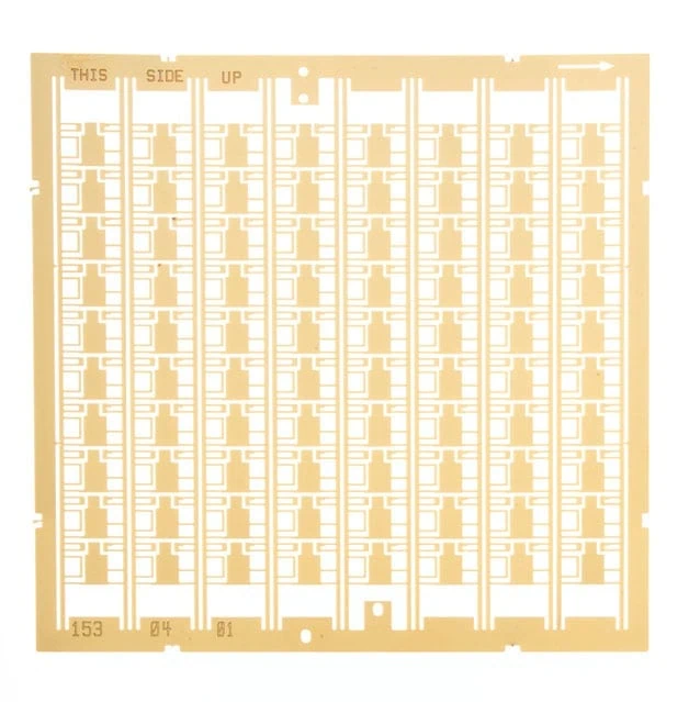
    Photo etched DBC circuit, photo etched direct bond copper

    Direct Bond Copper or DBC describes a ceramic substrate to which copper foil has been eutectically bonded to one or both sides. The most common and inexpensive ceramic is aluminum oxide, or alumina. For applications requiring higher currents and higher heat dissipation, aluminum nitride is used.

    The umbrella term “power electronics” refers to a range of semiconductor devices that are used to manage and manipulate the voltage, current and frequency of electric power. If it’s digital and has a battery, it needs a special semiconductor that maintains the correct operating voltage to the device regardless of the voltage state of the battery. If it’s digital and plugs into the wall, it needs a device to convert and step down the AC to DC. If you are charging a battery from an AC source, you need a semiconductor that converts the AC to DC at the correct voltage. If you are generating electricity from a variable source such as wind, solar, hydro, you need a semiconductor that converts the fluctuating AC to “clean” DC and then back to “clean” AC. Uninterruptible power supplies store DC power and output AC power. Common names for these types of devices include inverters, converters, and rectifiers. It’s all about managing and converting flows of alternating (AC) and direct (DC) current.

    Whenever you are dealing with the flow of electric current, you are also dealing with heat. Delicate electronics and heat are not a good combination.

    That’s where ceramics come in handy. They don’t conduct electricity and they are good at dissipating heat. When bonded to a good conductor of both current and heat, such as copper, ceramics provide additional heat dissipating capacity.

    Direct bond copper (DBC) is the go-to solution. The most widely used ceramic is aluminum oxide, or alumina, which has heat dissipating capacity up to about 48 w/mK (watts per meter*Kelvin.)  Aluminum nitride (AlN) can dissipate over 150 w/mK. Aluminum nitride is about 3 times the cost of alumina. In either case, typically .005?, .008?, or .012? thick wrought copper strip is eutectically bonded to one or both sides of the ceramic tile.

    The way to fabricate the DBC substrates into useful devices is to photo etch circuits into the copper. Chemical etching selectively removes the copper without affecting the ceramic in any way. The DBC substrates are frequently produced as approximately 5″ x 7″ tiles. The phototool is designed to replicate as many copies of the DBC circuit as will fit on the tile. The individual circuits are spaced to allow secondary fabricating processes after photo etching.

    After etching, additional fabricating steps include laser scribing and, often, hole drilling. The laser scribing allows the ceramic to be cleanly snapped into single circuits. Most often, the etched substrates are plated with electroless nickel and immersion gold, a process known as ENIG.

    The etched, scribed and plated substrates typically will have one or more surface mounted components wire bonded to the gold. After the components are assembled, the individual circuits are singulated and are ready for the next assembly process.

    DBC circuits are found in nearly every mobile device and a wide range of wireless communications products. As devices become smaller and more powerful, the need for DBC circuits to manage energy and heat becomes ever more important.

    Photo chemical etching is the most cost effective solution for processing direct bond copper substrates. It produces a crisp, clean circuit free of burrs or distortions. We have extensive experience etching DBC products for a wide variety of applications.

    Request Info on DBC

  2. Benefits of Working with an Outside Photo Etching Supplier

    Leave a Comment
    Automated Photo Etching Equipment

    Twenty-five or so years ago, the photo etching process was a lot more common in manufacturing, particularly for printed circuit boards. Back then, there were at least 100 companies, just in Connecticut, that etched circuit boards. Today, there are barely a handful and only a few hundred in the country. As pcb manufacturing migrated overseas, the knowledge base for photo etching declined.

    When there was a population of people who had etching experience, there were companies that decided to do their own etching. In those days, environmental requirements were less rigorous and the costs of waste management were much lower. Over the intervening years, things have changed quite significantly with regard to photo chemical etching.

    Today, environmental compliance costs, safety, and waste treatment and disposal are significant cost factors for etching. Interestingly, there are about the same number of commercial photo etching companies today as there were 25 plus years ago.

    In addition to shouldering the costs of the regulatory and environmental burdens, photo etching equipment is not a long-lived asset. Exposure to the etching solution, which is both heated and pressurized, takes its toll on the conveyors, bearings, and pumps. We routinely replace equipment every four years. If you are etching only part time, or intermittently, your etching equipment is degrading in place.

    There are eight reasons why you should be working with a commercial photo etching supplier rather than doing your chemical etching in house:

    1. Utility Costs:  chemical etching equipment uses a ton of power to run compressors, pumps, conveyors and sprayers. The etching process also uses a lot of water for regeneration, rinsing, developing and stripping.

    2. Chemistry and supply costs:  Etchant, developer, stripper and photoresist are significant elements in the cost of goods. And, if you are not etching on a continuous basis, those costs are not amortized efficiently.

    3. Waste treatment and disposal:  Even with on-site waste treatment, what and how much can be put down the drain is tightly regulated. Other wastes must be processed by regulated facilities and everything has to be accounted for and documented in perpetuity.

    4. Regulatory and compliance costs:  It’s not enough to follow the rules. You have to pay permit fees, audit fees, consulting fees, disposal fees and more, just for the fact of using photo etching as a manufacturing process. And, don’t forget the potential for fines if you have a problem.

    5. Maintenance and repair costs: Photo etching equipment requires regularly scheduled M&R, just like an airplane. After every so many hours of operation, there are parts that need to inspected, serviced or replaced. Keeping an etching line running for 4 years isn’t like keeping a refrigerator plugged in.

    6. Capital Expenses:  After keeping an etching line running for four years, you still have to replace it. Just write a check in the six-figure range.

    7. Training and Safety: There are state- and federally-mandated safety training requirements  for which a certified instructor is required. Every new employee must be trained to the requirements and every employee must complete retraining annually.

    8. Determining your true cost of goods:  Do you really know what your etching costs are?  It’s not just the cost of the metal. What about the defective parts you make?  What about unabsorbed overhead related to start up and shut down?  What about production efficiency? Can you run that equipment as productively as a full time facility?

    When you work with a commercial etching facility, all of these issues evapor

  3. Photochemical Etching with Ferric Chloride: Benefits and Drawback

    Leave a Comment

    Ferric chloride is the most widely used etchant for commercial chemical etching facilities. It is comparatively inexpensive, safe to use, consistent in etching performance, and versatile in etchable alloys.

    Fe3Cl is versatile and effective

    It is especially well-suited to etching the “white” metals, which include the iron- and nickel-based alloys, as well as zinc, manganese, indium and tin.The primary iron-based alloys include stainless, carbon and silicon steels. Kovar and Invar are iron-nickel alloys often used in etched electronics packaging applications. Alloys whose major fraction is nickel include Alloy 42, Inconel, and Mu-metal. Although ferric chloride will not directly each certain pure metals including cobalt, chromium and tungsten, these elements may be present up to certain fractions in iron or nickel alloys and they will be etched.

    Using ferric chloride to chemically etch white metals produces a smooth side wall with a consistent and predictable etch rate.

    For more details on the photo etching process and its capabilities, the Comprehensive Guide to Photochemical Machining is available for FREE:
    Download the Guide

    Etchant Regeneration Extends Service Life

    Another benefit to using ferric chloride is that it can be regenerated in process. Instruments within the etching process monitor the chemistry on a continuous basis. At specific thresholds, the etchant is refreshed by injections of muriatic acid, chlorine and water. In this way, the etchant bath life can be extended to several weeks.

    Even after several weeks of etching white metals, ferric chloride continues to be useful. It can be modified to be suitable for etching “red” metals. Red metals are copper based, and include primary coppers, brass, bronze, Monel, nickel silver (a copper alloy that actually contains no silver at all), and some specialty alloys. Again, the condition of the etchant is monitored automatically and refreshed as needed. In this way, the life of the original etchant is extended for several more weeks.

    After the ferric chloride has done its work etching white and red metals; it is reconfigured one more time to etch aluminum. Aluminum is a very light metal, about one-third of the density of the red and white alloys. It is also very reactive and wants to oxidize readily. The modified etchant is suited to this task.

    From an operational point of view, ferric chloride is fairly benign to work with. Casual exposure does not cause injury and is readily remedied with water. There are etching chemistries, both acid and alkaline, that will cause significant injuries on contact, and one –hydrofluoric acid, that can cause death. Ferric chloride has none of those risks.

    However, ferric chloride doesn’’t etch everything. In particular, the “noble” metals: gold, silver, platinum, palladium, tantalum won’t etch in ferric chloride. The so-called “high temp” metals: titanium, molybdenum, tungsten, cobalt, chromium, niobium also do not etch in ferric.

    We have alternative etchants that are effective for silver and molybdenum.

    Chemical Etching at the Atomic Level

    To explain how the etching process works requires a little trip back to high school chemistry class. The smallest particle of an element (such as iron, nickel, copper, aluminum, etc) is an atom. Atoms are composed of protons, neutrons and electrons.  Ions are atoms that have an unequal number of protons and electrons. Metals ionize by shedding electrons, making them into positively charged cations.  Non-metals ionize by gaining electrons and becoming negatively charged anions.

    Ferric chloride etching solution contains iron in the +3 oxidation state (meaning it has lost three of its 56 electrons) and chlorine with an extra electron forming the chloride Cl-. The etching process is essentially the deconstruction of the elements in the metal alloys at the atomic level. The cations gain electrons from the exposed metal atoms and then the anions bond to the exposed atomic nucleii.

    Photochemical Etching with Ferric Chloride: Benefits and Drawback

    These “non ferric” alloys can be etched with other solutions which are sometimes combinations of different acids like sulfuric, nitric, hydrochloric or phosphoric. Or, when the etching facility is especially equipped for containment and safety, hydrofluoric etches just about everything.

    Although regeneration and re-purposing of the ferric chloride etchant extends the life and usefulness of the etching solution, it does have a side effect. The process actually increases the overall volume of the etching solution by several times. After the etchant is consumed, the spent solution is neutralized. The dissolved metals are precipitated out and sent for refining and recycling. The remaining liquid, which is basically water, is treated and can be recycled as well.

    Request A Quote

    ADDITIONAL RESOURCES

    The Comprehensive Guide to Chemical Machining
    DOWNLOAD

    Introduction to Electroforming
    DOWNLOAD

    Design Considerations for Photo Etching
    DOWNLOAD

  4. What is the difference between Photo Etching and Metal Stamping?

    Leave a Comment
    Rawing of Photo Etched Stainless Steel Part

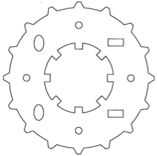
    This little part recently starred in Conard’’s new video about photo etching. “CC Star,” as we call it, is 2.7 inches in diameter and is .020” thick stainless steel. Just to satisfy our own curiosity, we asked other types of metal fabricators to quote this part.

    Metal Stamping

    The metal stamping company quoted about $10,000 to $13,000 to make the hardened steel tooling to produce CC Star. The lead time for the tooling was 6 weeks. The cost of the phototool we would use for etching would be $235. The lead time would be one day. So far, the difference between metal stamping and photo etching is $12,765 and 41 days.

    The stamping tool is kind of a big deal. Just the steel, wire EDM service and heat treating for this particular part will run between $6,000 and $9,000. The tool maker figures between 80 and 100 hours of labor for prep and assembly. A die-maker’s time is worth $60-$80 per hour. So, a rather strenuous undertaking to produce a smallish metal part.

    Once the stamping tool is complete, it needs to be set up in a stamping press. If the stamping house has adopted SMED practices (Single Minute Exchange of Dies), the installation and alignment can be done fairly quickly. It could also be a more involved process…. Once the tool is installed, set up pieces are run and the press is adjusted to produce the parts correctly.

    Chemical Etching

    To produce the phototool, the designer takes our CAD file and adjusts the dimensions to account for the etching allowance. It’s a formulaic process where outside dimensions are made a little bigger and inside dimensions are made a little smaller by a ratio related to the metal thickness. The designer then adds connecting tabs, if required. This “compensated” image is stepped-and-repeated to fill a designated sheet of material. In this case, we chose an 18” x 24” sheet, which allows us to etch 48 parts per sheet. The resulting file is output to a laser photoplotter to produce 2 sheets of film at 8000 dpi resolution. The 2 films are precision aligned and punched for registration. End to end, the process takes about 2 hours, including the plotter time.

    The photo tool requires no set up. The bottom sheet is placed on the registration pins in the vacuum frame. The resist-coated sheet of metal is placed on top of it and butted against the registration pins. The top sheet of the tool is placed on the registration pins. The frame is closed and squeegeed; a vacuum is drawn and the plate is exposed. The cycle time is one minute.

    Cycle Times

    When the stamping press is released for production, they can make about 40 parts per minute….all day long. So, in an 8 hour shift, they can make about 20,000 parts.

    In photo etching, after the plate is exposed in printing, the sheets are sent through developing where the unexposed resist is washed away. The developed sheets go into the etching line, one after the other, making about 800-850 parts per hour. 6,400 or so parts per 8 hour shift.

    For CC Star, laser cutting can produce about 80 parts per hour and waterjet makes about 30 parts per hour.

    From a tooling and process standpoint, the photo etching and stamping processes are very different.

    Let’s look at the cost differences between chemical etching and metal stamping.

    Here’s the price comparison for CC Star produced in .020” stainless steel:

    Photo EtchingMetal StampingLaser CuttingWater Jet
    Tooling$235$10-$13,000N/AN/A
    Cycle Time850 Pcs/Hr2400 Pcs/Hr80 Pcs/Hr30 Pcs/Hr
    1000 pcs$2.03$3.85$2.03$3.50
    5000 pcs$1.96$1.95NQNQ
    10000$1.81$1.80

    In this particular case, due to the complexity of the part, the amortization of the stamping die expense would require up to 1.3 million parts to be made.

    If you are ready to find out how your application compares:

    Request A Quote

    ADDITIONAL RESOURCES

    The Comprehensive Guide to Chemical Machining
    DOWNLOAD

    Introduction to Electroforming
    DOWNLOAD

    Design Considerations for Photo Etching
    DOWNLOAD

  5. How to Avoid Design Problems in Photo Etching

    Leave a Comment
    Photo Etched Microelectronics Leadframe

    The biggest design problem is that the design requirements for photo etching are not widely understood. The five most common etching design problems are:

    1. Choosing metal that is thicker than needed

    Specifying material thickness in excess of what the application requires. It is not uncommon to see drawings asking for much heavier gauges of metal than the part’s function may require. Frequent situations include parts that do not have functional or structural roles being designed with 18 or 20 gauge steel because the designer thought it was common. Heavier gauges are common in sheet metal applications, but are not suited to photo etching. In stainless or carbon steel, 20-gauge (about .036”) is the upper limit. In aluminum sheet, the photo etching process can handle up to 12-gauge (.080”). In copper sheet, the etching limit would be 14-gauge (.065”). Understand that with every mil (.001”) of thickness comes another fixed increment of etching time. Use the lightest material suitable for the process.

    2. Making tolerances tighter than needed

    Although the metal etching process can generally achieve +/-15% of the metal thickness, tighter tolerances affect costs. +/-.0015” is the minimum absolute tolerance and can only be achieved if the metal is .010” thick or less. +/-.005” is suitable for metal thicknesses up to .030”. Tolerances for thicker materials will be +/-20% of the metal thickness. The tighter the tolerance band, the smaller the sheet size, and the higher the costs. The economies of photo etching are best realized by being as generous as possible with tolerances. Location tolerances are defined by the CAD data and will consistently be +/-.001” to drawing nominal.

    3. Designing features (holes, slots, ligaments) that are too small for the metal thickness

    Metal thickness also defines minimum feature sizes in photo etching. The minimum dimension for etching holes is at least 110% of metal thickness. The photo etching process uses etching solution to dissolve the metal to be removed. In order to etch all the way through the metal, there needs to be enough space for the etchant to flow. Similarly, the land area between holes needs to be at least equal to the metal thickness. The reason here is that the etchant will undercut the photo resist and cause the land area to be etched away.

    4. Ignoring industry standards for metal gauges and tolerances

    Another problem we encounter with customer designs is lack of attention to industry standards with regard to raw material. Strip metals are generally rolled to a thickness tolerance of +/- 10% of the nominal. Precision stainless strip is available at +/-5% of nominal. Drawing call outs that are tighter than industry norms can lead to a lot of excess cost. Many alloys can be precision rolled to +/-.0001” on thickness, but expect to pay upwards of $1000 per pound and wait 12 weeks for it. There is no industry standard for flatness of rolled metals, even for tension leveled material. This applies to all rolled metals, not just for photo etching.

    5. Not checking metal availability before specifying

    In the wake of the 2008/2009 economic downturn, the metal making industries sharply “rationalized” their production. Gone were the days of running 50,000 pounds of a particular alloy or gauge that would take 20 years to sell through. That was a pretty painful lesson for many.

    In the wake of the 2020 pandemic, the  further “rationalization” of production plans and inventories has narrowed the product selection even further.

    There are many more alloys covered by standards than are being made. In the past 5 years alone, the stock situation for raw materials has been significantly rationalized both at the distribution levels and at the mills.

    The mills will still make whatever you want, but you won’t like the cost or the minimum weight. It becomes a major challenge when a legacy part for a prime contractor is calling for what we call “un-obtainium.” Before specifying an alloy based on its data sheet, contact us to see if it’s really available.

     “When you want to stop digging a hole; the first rule is to put down the shovel.”–Anon

    These are the five most frequent problems we see with new designs being considered for photo etching. One of the reasons we’re here is to answer those questions before they become specifications.

    The simple solution: Talk to us first!

    New Call-to-action
  6. What are the most common design problems in Photo Etching?

    Leave a Comment
    Photo Etched Microelectronics Leadframe

    The biggest design problem is that the design requirements for photo etching are not widely understood. The five most common etching design problems are:

    Specifying material thickness in excess of what the application requires. It is not uncommon to see drawings asking for much heavier gauges of metal than the part’s function may require. Frequent situations include parts that do not have functional or structural roles being designed with 18 or 20 gauge steel because the designer thought it was common. Heavier gauges are common in sheet metal applications, but are not suited to photo etching. In stainless or carbon steel, 20-gauge (about .036”) is the upper limit. In aluminum sheet, the photo etching process can handle up to 12-gauge (.080”). In copper sheet, the etching limit would be 14-gauge (.065”). Understand that with every mil (.001”) of thickness comes another fixed increment of etching time. Use the lightest material suitable for the process.

    Although the metal etching process can generally achieve +/-15% of the metal thickness, tighter tolerances affect costs. +/-.0015” is the minimum absolute tolerance and can only be achieved if the metal is .010” thick or less. +/-.005” is suitable for metal thicknesses up to .030”. Tolerances for thicker materials will be +/-20% of the metal thickness. The tighter the tolerance band, the smaller the sheet size, and the higher the costs. The economies of photo etching are best realized by being as generous as possible with tolerances. Location tolerances are defined by the CAD data and will consistently be +/-.001” to drawing nominal.

    Metal thickness also defines minimum feature sizes in photo etching. The minimum dimension for etching holes is at least 110% of metal thickness. The photo etching process uses etching solution to dissolve the metal to be removed. In order to etch all the way through the metal, there needs to be enough space for the etchant to flow. Similarly, the land area between holes needs to be at least equal to the metal thickness. The reason here is that the etchant will undercut the photo resist and cause the land area to be etched away.

    Another problem we encounter with customer designs is lack of attention to industry standards with regard to raw material. Strip metals are generally rolled to a thickness tolerance of +/- 10% of the nominal. Precision stainless strip is available at +/-5% of nominal. Drawing call outs that are tighter than industry norms can lead to a lot of excess cost. Many alloys can be precision rolled to +/-.0001” on thickness, but expect to pay upwards of $1000 per pound and wait 12 weeks for it. There is no industry standard for flatness of rolled metals, even for tension leveled material. This applies to all rolled metals, not just for photo etching.

    The overall availability and variety of metals has changed. There are many more alloys covered by standards than are being made. In the past half dozen years alone, the stock situation for raw materials has been significantly rationalized both at the distribution levels and at the mills. The mills will still make whatever you want, but you won’t like the cost or the minimum weight. It becomes a major challenge when a legacy part for a prime contractor is calling for what we call “un-obtainium.” Before specifying an alloy based on its data sheet, contact us to see if it’s really available.

    These are the five most frequent problems we see with new designs being considered for photo etching. One of the reasons we’re here is to answer those questions before they become specifications.

    In shorthand, the five design mistakes to avoid in photo etching are:

  7. How do Photo Etching and Laser or Water Jet Cutting Compare?

    Leave a Comment
    Photo Etched Stainless Steel

    This little part recently starred in Conard’s new video about photo etching. “CC Star,” as we call it, is 2.7 inches in diameter and is .020” thick stainless steel. Just to satisfy our own curiosity, we asked other types of metal fabricators to quote this part.

    Laser and water jet cutting technologies are fast, flexible digital solutions for cutting metals and a variety of materials. Lasers use combinations of collimated light and gas to burn a path through material. Water jets use either pure water under very high pressure or a slurry of water and abrasive to scour a path through material. In both cases, digital controls guide the cutting heads. And, in both cases, the cutting beam must trace all of the features of the part in a linear fashion as if you were tracing with a pencil. (As a practical matter, the cutting paths are often segmented, but the entire path must be covered.)

    Neither lasers nor waterjets require hard tooling. Both require programming, which is a simple matter of software these days. While lasers are generally faster than waterjets, the actual cutting speeds of both technologies is dependent on a number of factors: type and thickness of material, size and shape of the part, tolerances required, and the power of the equipment itself.

    In .020” stainless, CC Star might take 2 or so minutes on a waterjet and about 45 seconds on a laser.

    Photo etching requires what is sometimes referred to as “soft tooling”. Phototools are images of the parts on film. At the beginning, the process of preparing the tooling information is similar to the programming of a laser or waterjet.

    To produce the phototool, the designer takes our CAD file and adjusts the dimensions to account for the etching allowance. This “compensated” image is stepped-and-repeated to fill a designated sheet of material. In this case, we chose an 18” x 24” sheet, which allows us to etch 48 parts per sheet. The resulting file is output to a laser photoplotter to produce 2 sheets of film at 8000 dpi resolution. The 2 films are precision aligned and punched for registration. End to end, the process takes about 2 hours, including the plotter time.

    After printing and developing, the metal sheets go into the etching line, one after the other, making about 800-850 parts per hour, regardless of how complex the part is.

    By comparison, to produce CC Star, a water jet would run 50 or so parts per hour and a laser about 100 parts per hour.

    In 1000 piece quantities, the etched part costs $2.03. Waterjet was quoted at $3.50. And laser cutting is $2.04.

    When part geometries are complex, photo etching is the better choice because the rate of production is not affected. If the part had been a simple disk, etching throughput and cost would be exactly the same. For the same size disk, the throughput rates for lasers and waterjets would be faster.

    Awareness of laser and water jet cutting is widespread. There are more than 6,000 metal fabricators in the US; the vast majority of which utilize digital cutting technologies. Despite its emergence in the 1950s as means of fabricating metal parts, and long before the digital age, photo chemical etching is still a little known process. There are barely 100 etching companies in the US and only a few hundred in the world. Photo etching is very capable of working with the very thin materials and fine design details that  are in growing demand in a range of industries.

    If you have any questions about photo etching, please contact me at 800-443-5218 or click below to email me.

  8. Photo Chemical Etching vs the MetalPhoto Process?

    Leave a Comment
    Stainless Steel Sign Etched and Color Filled

    MetalPhoto Has No Etching At All

    MetalPhoto® is the registered trademark for a product and process produced by Horizon Imaging Systems Group. The basis of the technology is silver halide coated aluminum topped by clear anodize. Silver halide is a photo sensitive emulsion that was widely used in photographic film, which turns opaque black when exposed to light and developed.

    The only similarity between MetalPhoto and photo etching is that both processes rely on a phototool as an exposure mask. After exposure, the MetalPhoto plate is processed in a developer/fixer solution and then sealed in another solution. The primary applications for MetalPhoto are nameplates, metal labels for bar codes, identification, instructions, warnings and so forth. Fabrication of the finished parts by ordinary metal cutting methods occurs after the images have been developed and sealed. There is no actual chemical etching involved. The MetalPhoto process is specified under MIL-STD 130N. The process is often used by nameplate and identification products manufacturers.

    Photo Etching is a Metal Fabrication Process

    Photo chemical etching is a method of fabricating precision metal parts by using acid to “machine” the metal. Also known as photochemical machining (PCM), the process is ideally suited for small, intricate parts made of flat metal. The chemical etching process (yet another name…) is a frequent alternative for stamping as the tooling is inexpensive and can be made in a day.

    Photo etching (a shorter version…) is also capable of very fine detail which cannot be stamped and is able to produce slots and holes as small as 110% of the thickness of the metal being etched. Photo etching uses no oils so parts are never contaminated with lubricants, and the process is completely compatible with requirements of RoHS.

    Photo etching is also used to produce durable metal graphics with color fill. Unlike Metalphoto graphics, which are not etched at all, photo etched graphics are typically .010” to .032” deep and color filled with durable epoxy or powder coat.

    Because graphics are etched only on one side of a plate, heavier gauges of metal can be used. Durable metal graphics are etched on metal plates from 11 gauge (.12”) to 20 gauge (.048”). These plates are either pre-cut to size before etching or sheared to size after etching. Photo etching is capable of producing ADA-compliant braille and symbols.

    Photo chemical etching is used to produce a wide variety of decorative, giftware and jewelry items along with graphics and branding items. Etched kits for scale models are produced for railroads, ships and so forth.

    The same ability to etch graphics from one side is frequently used to incorporate surface designs onto many decorative pieces. The method is deceptively simple. Since the etching through process occurs from both sides of the metal simultaneously, the decorative detail appears on only the top side of the phototool.

    There are two ways to get half etch surface detail on both sides of a plate. Understand that when images on the top and bottom halves of a photo tool line up, you get a hole. If you are very clever and exacting in your design to insure that decorative detail on the top half of the tool never coincides with detail on the bottom half of the tool, you can get half etched detail on both sides.

    The usual way to etch surface detail on both sides, however, is to use double process. Double process uses a four-piece photo tool set, instead of the usual 2 piece set. And, then we do everything twice, except cut the metal. The first process etches the surface detail, typically .002-.004” deep on both sides. The partially etched plate is stripped, relaminated with resist and then imaged with the cut-through

    For more information, get our FREE Comprehensive Guide to Photo Etching:

    Download the Guide
  9. What Effect does Sheet Size have on the Cost of Photo Etching?

    Leave a Comment
    What Effect does Sheet Size have on the Cost of Photo Etching?

    The two biggest variables affecting the cost of photo etching are metal thickness and sheet size. Metal thickness bears directly on the length of time it takes to etch through a given metal thickness measured in minutes per mil (.001”) of thickness. Sheet size drives the amount of labor that accumulates.

    The photo etching process has seven essential steps: cutting, cleaning, laminating, printing, developing, etching and stripping. For each of these steps, a sheet of material must be handled. Each time a sheet is handled into and out of a step in the photo etching process, labor is applied. If you were loading and unloading a pizza oven, your hands wouldn’t care if it was a small pizza or a large pizza. You can easily see that loading and unloading many small sheets (pizzas) consumes more labor than handling a smaller number of large sheets.

    The effect of sheet size on the cost of photo etching is illustrated in the table below:

    The “test part” is a 1” x 1” x.010” thick part. It doesn’t make any difference whether the part is a simple disk (cheese pizza), a washer (pepperoni pizza), a spring form (pepperoni, sausage and mushrooms), or a screen (the “works”). The photo etching process doesn’t care.

    Prices shown do not include any material cost.

    Sheet Size12 x 1212 x 1812 x 2418 x 24
    Min Tolerance+/-.002+/-.0025+/-.003+/-.004
    500.59.43.41.38
    1000.56.39.36.31
    2500.52.38.29.25
    5000.45.33.29.23
    10000.42.31.27.22
    25000.40.30
  10. What Does Photo Etching Cost?

    Leave a Comment

    Key Elements of Etching Costs

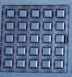
    Photo Etched Spectroscopy Grids

    Like any other manufacturing process, chemical etching costs are the sum of a number of elements. The most variable cost elements in photo etching are: metal and photoresist, labor, and machine time. The indirect costs consist of etching chemistries including developer, etchant and stripper. Power, water and waste treatment are figured into the overhead cost rate.

    Main Materials: Metal and Resist

    Considering alloy and thickness, metal costs vary widely. Common alloys and gauges of copper, steel, or aluminum might run between $5 and $10 per pound. Thinner materials cost more per pound: .001” thick stainless is about $50 per pound. However, .0005” stainless costs more than $100 per pound. Beryllium copper is around $35 per pound. Molybdenum is more than $150 per pound. The cost of photoresist is a constant value per square inch.

    Request A Quote

    Larger Sheets Reduce Labor per Unit

    The unit of labor in photo etching is the sheet. There are seven manufacturing operations during which labor is accumulated: cutting, cleaning, laminating, printing, developing, photo etching and stripping. Each of these steps requires that the sheet be handled into and out of the operation. The amount of labor required is fairly consistent per sheet, regardless of the size of the sheet. Indirect labor is applied in inspection and packaging.

    In most cases, smaller sheets accumulate labor at essentially the same rate as the larger sheets. The application of labor is relatively indifferent to the sheet size. So the sheet size is an important factor in photo etching costs.

    Machine time costs accumulate in cleaning, developing, photo etching and stripping. During machine time, multiple sheets are transported by conveyors at speeds determined by the processing requirements. The etching process itself is the slowest, usually running at a few minutes per inch of travel.

    We measure capacity at each step in “sheets per hour,” which takes into account both the labor and the machine time. Each work step has a through-rate based on sheet size. The through-rate in the etching process is based on sheet size, alloy and metal thickness. Metal alloys etch at known rates per mil (.001”) of thickness so the required duration of the exposure to the etching chemistry is predictable.

    Dimensional Tolerances Drive Sheet Size

    Dimensional tolerances also affect the sheet size for photo etching as the tolerance variance from the center of the sheet to the edges increases with the distance. So, even a simple part with tight tolerances might have to be produced on a very small sheet. Tight tolerances also affect etching costs because the production yield of parts within tolerance decreases.

    With just a little information, we can give you an estimate for photo etching your parts. The Instant Estimate feature at the top of every page at www.conardcorp.com is intended to provide that type of information as quickly as we can. With just 5 bits of information: length, width, thickness, alloy and quantity, we will provide an estimate for photo etching your parts in as little as minutes. For a firm quote, we need an engineering spec that includes exact dimensions and tolerances.

    You can do that here:

    Request A Quote

    ADDITIONAL RESOURCES

    The Comprehensive Guide to Chemical Machining
    DOWNLOAD

    Introduction to Electroforming
    DOWNLOAD

    Design Considerations for Photo Etching
    DOWNLOAD