Typically produced from silicon steel alloys, also referred to as “electrical” steel or “M series” that have a surface finish called “coreplate” which creates a dielectric layer between laminations.
Metal etching is an ideal solution for small to mid-range (dozens to many thousands) quantities of rotor and stator lams for motors and “I”, “U” and “T” transfomer laminations.
Complex designs are easily produced from inexpensive tools (about $265.)
The chemical etching process leaves no burrs and imparts no mechanical or thermal stress: annealing is not needed.
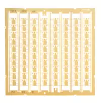
Microelectronics Packaging
Photo etching is the ideal solution for QFN and LD-MOS leadframes as well as a wide range of custom platforms.
QFN or “air-cavity” packages are widely used in RF and microwave communications applications due to the low attenuation loss. These leadframes are typically very complex and delicate designs that are well suited to the capabilities of chemical etching.
Flat and step lids for hermetically sealed electronics packages are also readily produced by photochemical etching. Common alloys for these applications are often in the nickel-iron family and include Kovar, Invar, F-15, and others.
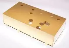
EMI/RFI Shielding
Many electrically “noisy” products emit interference which must be contained by metal shielding in copper, beryllium copper, brass and others.
Chemical etching is a fast and economical means of producing both simple and complex enclosures and barriers to electromagnetic and radio frequency emissions.
Pictured is an example of an etched and formed enclosure for electronic assemblies.
Direct Bond Copper is another popular application for photo etching. A layer of copper is vacuum bonded onto an alumina ceramic base and a circuit is etched into the copper. Etched DBC parts are used in many RF/microwave applications including cell phones, wireless and and microwave transmitters.